Diferență între revizuiri ale paginii „CID Seminar EN”
Cbira (discuție | contribuții) |
Cbira (discuție | contribuții) |
||
| (Nu s-a afișat o versiune intermediară efectuată de același utilizator) | |||
| Linia 43: | Linia 43: | ||
# It's the only signal in a digital system that's active on the front. All other signals present in a digital system are active on the floor. | # It's the only signal in a digital system that's active on the front. All other signals present in a digital system are active on the floor. | ||
| − | <div class = "rule"> The simplest way that a clock signal can be generated in Verilog is by using an ''''''''' | + | <div class = "rule"> The simplest way that a clock signal can be generated in Verilog is by using an '''initial''' prcess and '''forever''' loop. No instruction is added after the instruction ''forever'', because it will never run. </div> |
== Exercise 3 == | == Exercise 3 == | ||
| Linia 109: | Linia 109: | ||
<u> Additional explanations </u> | <u> Additional explanations </u> | ||
| − | The difference between the blocking and the non-blocking assignment types is | + | The difference between the blocking and the non-blocking assignment types is the following: unlike the blocking assignment (=), the non-blocking assignment (<=) does not immediately update the left regression signal, but only at the end of the current simulation step. |
| + | |||
| + | Here's an example: description of multiple bistables in different processes using the blocking assignment: | ||
| + | <syntaxhighlight lang = "verilog"> | ||
| + | always @ (posedge clock) | ||
| + | b = a; | ||
| + | always @ (posedge clock) | ||
| + | c = b; | ||
| + | </syntaxhighlight> | ||
| + | In this particular case, upon the arrival of a positive front of the clock in the simulation both processes are executed. However, it is impossible to say what will be the first process executed by the simulator. Two possible cases arise: | ||
| + | |||
| + | - Either the two processes are executed in the order in which they were written. In this case B will be updated the first and new value of B will be used to update it on C. So B and C will have the same value, namely the value A! | ||
| + | |||
| + | - Either the two processes will always be executed in the reverse order. In this case, C will be assigned the old value of B, then B will be updated with the value A. | ||
| + | |||
| + | Thus, differences between simulation results can occur with different simulation tools, but there may also be differences between RTL description simulation and post-layout simulation! | ||
| + | Here's what happens if we implement the two bistabs using non-blocking attributes: | ||
| + | <syntaxhighlight lang = "verilog"> | ||
| + | always @ (posedge clock) | ||
| + | b <= a; | ||
| + | always @ (posedge clock) | ||
| + | c <= b; | ||
| + | </syntaxhighlight> | ||
| + | In this case, B and C do not receive new values until after both assignments have been executed, ie on the next positive front! Thus, the schematic to be simulated will be the same as that generated by the synthesis of the RTL code. | ||
| + | |||
| + | Assignment == == | ||
| + | |||
| + | # Describe in Verilog a full counter (in, reset, load, enable, up / down, out). Simulate the operation of this counter. Consider 4-bit inputs. Highlight waveforms on the counter's output! What do you notice? | ||
| + | # Describe and simulate the operation of a left-hand drive using the << and concatenation arrow {}. | ||
| + | # Describe and simulate the operation of a circular left shift register (MSB becomes LSB). | ||
Versiunea curentă din 5 aprilie 2018 08:22
In this seminar you will learn what is a secession circuit and how it is described in Verilog.
Keywords:clock,flip-flop, blocking/non-blocking'
Verilog syntax: always, initial, forever
The digital circuits are of two types:
- Combinational logic circuits (CLC) - can be described either using 'assign' or using '
- sequential circuits - can be described using only always
Exercise 1
Describe in Verilog a bistable D with the following features:
- active clock signal on the positive front
- synchronous reset signal with the clock, active on the 0 scale
Additional explanation
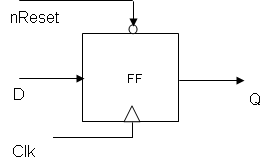
The most commonly used circuit to synchronize any clock signal is the flip-flop D (also called flip-flop FF). The binary D in this example has the following ports:
- Clk - clock input, active on the positive front
- D - Data entry
- nReset - synchronous clock signal input; nRest active on the 0 field
- Q - circuit output
Remark: The reset signal will always be synchronous with the clock, ie it will change its value from 1 to 0 or vice versa always on the active front of the clock !!!
The description of a RTL verilog in Verilog is only possible using always-type processes, with the sensitivity list at least the positive clock face.
In clock processes, signal values are assigned using the non-blocking assignment (with the operator <=, which in this context means "takes the value", and NOT less than or equal !!!) unlike the processes' always' that describe purely combinational circuits and where assigning new values is done using only the blocking assignment (with operator =).
Exercise 2
Simulate the operation of the bistable D. At the CK input a periodic signal with a period of 6 time units will be applied.
Additional explanation
The clock signal has the following properties:
- Rectangular signal (like all other digital signals)
- It's a regular signal
- It's the only signal in a digital system that's active on the front. All other signals present in a digital system are active on the floor.
Exercise 3
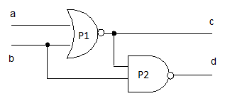
The combination circuit in the following figure has a hazard on the output. Describe this circuit in Verilog using a 'assign' statement and an 'always' process and then simulate its operation to highlight the hazard.
Additional explanation
When you use assign - the signal must be declared 'wire' '.
When using alwaysthe signal must be declared.
The hazard (behavior of combinational circuits that is not in accordance with logical algebra) is due to propagation times through logical gates. To highlight this phenomenon, we will introduce the propagation times through gates with the syntax: assign #tp ..., where tp is the propagation time.
Exercise 4
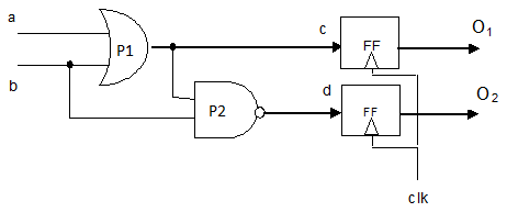
Describe the circuit in the following figure in Verilog and simulate its operation.
Additional explanation
The circuit can be described in two ways:
- separating the combined side from the sequential (using 2 processes always)
- using a single process always
The simulation will highlight the elimination of the hazard on the output.
Exercise 5
Simulate and compare the operation of the following circuits (in the two modules only the type of assignment used: non-blocking or blocking):
Circuit 1:
always @ (posedge clk) begin
    if (nReset == 0) begin
        b <= 0;
        c <= 0;
    end else begin
        b <= a;
        c <= b;
    end
end
Circuit 2:
always @ (posedge clk) begin
    if (nReset == 0) begin
        b = 0;
        c = 0;
    end else begin
        b = a;
        c = b;
    end
end
Note: This example will help you understand the above rule: Always use the non-blocking assignment <= to describe synchronous clock circuits.
Additional explanations
The difference between the blocking and the non-blocking assignment types is the following: unlike the blocking assignment (=), the non-blocking assignment (<=) does not immediately update the left regression signal, but only at the end of the current simulation step.
Here's an example: description of multiple bistables in different processes using the blocking assignment:
always @ (posedge clock)
    b = a;
always @ (posedge clock)
    c = b;
In this particular case, upon the arrival of a positive front of the clock in the simulation both processes are executed. However, it is impossible to say what will be the first process executed by the simulator. Two possible cases arise:
- Either the two processes are executed in the order in which they were written. In this case B will be updated the first and new value of B will be used to update it on C. So B and C will have the same value, namely the value A!
- Either the two processes will always be executed in the reverse order. In this case, C will be assigned the old value of B, then B will be updated with the value A.
Thus, differences between simulation results can occur with different simulation tools, but there may also be differences between RTL description simulation and post-layout simulation! Here's what happens if we implement the two bistabs using non-blocking attributes:
always @ (posedge clock)
    b <= a;
always @ (posedge clock)
    c <= b;
In this case, B and C do not receive new values until after both assignments have been executed, ie on the next positive front! Thus, the schematic to be simulated will be the same as that generated by the synthesis of the RTL code.
Assignment == ==
- Describe in Verilog a full counter (in, reset, load, enable, up / down, out). Simulate the operation of this counter. Consider 4-bit inputs. Highlight waveforms on the counter's output! What do you notice?
- Describe and simulate the operation of a left-hand drive using the << and concatenation arrow {}.
- Describe and simulate the operation of a circular left shift register (MSB becomes LSB).


