Diferență între revizuiri ale paginii „DIC Lab Work 1”
Cbira (discuție | contribuții) (Pagină nouă: == Notions and Knowledge Required == * Using the Altera Quartus II Synthesis Program * [http://wiki.dcae.pub.ro/images/f/fc/Pini_la_care_sunt_conectati_d...) |
|||
| (Nu s-au afișat 10 versiuni intermediare efectuate de alți 2 utilizatori) | |||
| Linia 1: | Linia 1: | ||
== Notions and Knowledge Required == | == Notions and Knowledge Required == | ||
| − | * [[ | + | * [[Quartus_II_tutorial | Using the Altera Quartus II Synthesis Program]] |
* [http://wiki.dcae.pub.ro/images/f/fc/Pini_la_care_sunt_conectati_dispozitivele_I-O_pe_placa_experimentala_DE1.pdf List of pins for plate DE1] | * [http://wiki.dcae.pub.ro/images/f/fc/Pini_la_care_sunt_conectati_dispozitivele_I-O_pe_placa_experimentala_DE1.pdf List of pins for plate DE1] | ||
* [http://wiki.dcae.pub.ro/images/d/d9/Lista_pinilor_pl%C4%83cii_DE1-SoC.pdf Plate pin list DE1_SOC] | * [http://wiki.dcae.pub.ro/images/d/d9/Lista_pinilor_pl%C4%83cii_DE1-SoC.pdf Plate pin list DE1_SOC] | ||
| − | * [[Introduction. | + | * [[Introduction._Verilog_HDL_(Verilog_syntax)#Numbers_and_symbols._Numbering_Bases|Boolean logic and numbering systems]] |
* Syntax notions [[Verilog]] | * Syntax notions [[Verilog]] | ||
| Linia 14: | Linia 14: | ||
<syntaxhighlight lang="Verilog"> | <syntaxhighlight lang="Verilog"> | ||
| − | OrGate | + | module OrGate( |
output out, | output out, | ||
input in1, | input in1, | ||
input in2 | input in2 | ||
| − | ) | + | ); |
assign out=in1 | in 2; | assign out=in1 | in 2; | ||
endmodule | endmodule | ||
| − | <syntaxhighlight> | + | </syntaxhighlight> |
Add the necessary constraints for the circuit's inputs and outputs to be connected as follows: | Add the necessary constraints for the circuit's inputs and outputs to be connected as follows: | ||
| Linia 32: | Linia 32: | ||
Implement the project on the DE1 board and observe the circuit functionality described by the Quartus II project. | Implement the project on the DE1 board and observe the circuit functionality described by the Quartus II project. | ||
| − | The list of pins to which I /O devices are connected to the DE1 board are described [http://wiki.dcae.pub.ro/images/f/fc/Pinii_la_care_sunt_conectati_Dispozitivele_I-O_pe_placa_experimentala_DE1.pdf here] | + | The list of pins to which I /O devices are connected to the DE1 board are described |
| + | [http://wiki.dcae.pub.ro/images/f/fc/Pinii_la_care_sunt_conectati_Dispozitivele_I-O_pe_placa_experimentala_DE1.pdf here] | ||
| + | and to the DE1-SoC | ||
| + | [http://wiki.dcae.pub.ro/images/3/37/Pin_Assignments_Cyclone_V_.pdf here] | ||
== Exercise 1 == | == Exercise 1 == | ||
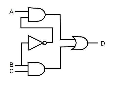
| − | + | Implement the Verilog description of the module with the inputs '''a''', '''b''', '''c''' and the output '''d''' with the functionality shown in the diagram below. Implement the circuit on the DE1/DE1-SoC board by connecting inputs a, b, c to SW2, SW4, and SW6 respectively, and output d to LEDR2. | |
[[File: lab1_ex1.jpg]] | [[File: lab1_ex1.jpg]] | ||
| Linia 42: | Linia 45: | ||
== Exercise 2 == | == Exercise 2 == | ||
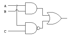
| − | + | Implement the verilog description of the module with the inputs '''a''', '''b''', '''c''' and the output '''q''' with the functionality in the diagram below. Implement the circuit on the DE1/De1-SoC board by connecting inputs a, b, c to SW3, SW4, and SW7, and output q to LEDR7. | |
[[File: lab1_ex2.gif]] | [[File: lab1_ex2.gif]] | ||
| Linia 48: | Linia 51: | ||
== Exercise 3 == | == Exercise 3 == | ||
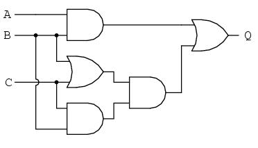
| − | + | Implement the verilog description of the module with the inputs '''a''', '''b''', '''c''' and the output '''q''' with the functionality in the diagram below. Implement the circuit on the DE1/De1-SoC board by connecting inputs a, b, c to SW1, SW6, and SW7, and output q to LEDR3. | |
[[File: lab1_ex3.jpg]] | [[File: lab1_ex3.jpg]] | ||
| Linia 54: | Linia 57: | ||
== Exercise 4 == | == Exercise 4 == | ||
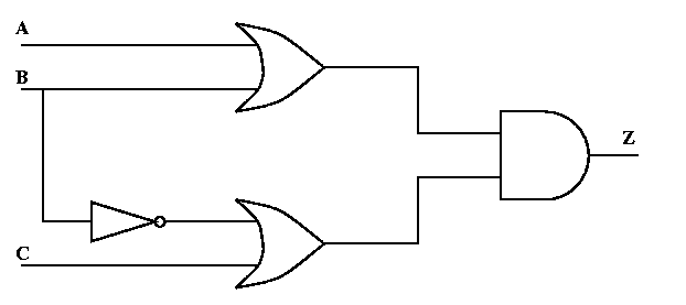
| − | + | Implement the description in Verilog of the module with the inputs '''a''', '''b''', '''c''' and the output '''z''' with the functionality in the diagram below. Implement the circuit on the DE1/De1-SoC board by connecting inputs a, b, c to SW3, SW4, and SW5, and output z to LEDR6. | |
[[File: lab1_ex4.png]] | [[File: lab1_ex4.png]] | ||
| Linia 60: | Linia 63: | ||
== Exercise 5 == | == Exercise 5 == | ||
| − | + | Implement the Verilog description of the module with the inputs '''a''', '''b''', '''c''' and the output '''y''', with the functionality in the diagram below. Implement the circuit on the DE1/De1-SoC board by connecting inputs a, b, c to SW5, SW6, and SW7 respectively, and output y to LEDR4. | |
| − | [[File: lab1_ex5.png]] | + | [[File: lab1_ex5.png|center|300px]] |
== Exercise 6 == | == Exercise 6 == | ||
| − | + | Implement the Verilog description of the module with the inputs '''a''', '''b''', '''c''' and the output '''y''', with the functionality in the diagram below. Implement the circuit on the DE1/De1-SoC board by connecting inputs a, b, c to SW5, SW4, and SW1, and output y to LEDR7. | |
| − | [[File: lab1_ex6.png]] | + | [[File: lab1_ex6.png|center|400px]] |
== Submission of Exercise Solving == | == Submission of Exercise Solving == | ||
| Linia 85: | Linia 88: | ||
== Recommendations for Teachers == | == Recommendations for Teachers == | ||
| − | * Implementing a Quartus project example, going through the [[ | + | * Implementing a Quartus project example, going through the [[Quartus_II_tutorial | tutorial]]. |
Versiunea curentă din 24 februarie 2019 15:29
Notions and Knowledge Required
- Using the Altera Quartus II Synthesis Program
- List of pins for plate DE1
- Plate pin list DE1_SOC
- Boolean logic and numbering systems
- Syntax notions Verilog
Example
Create a new project in Quartus II for the Altera Cyclone II FPGA on the DE1 board. Create a Verilog source file within the project, and copy the next module to the file.
Warning! The name of the top-level module to be synthesized should be set correctly when you create the project (in this case, OrGate).
module OrGate(
output out,
input in1,
input in2
);

assign out=in1 | in 2;

endmodule
Add the necessary constraints for the circuit's inputs and outputs to be connected as follows:
- in1 connected to SW0: PIN_L22
- in2 connected to SW7: PIN_M2
- Out connected to LDR3 (red LED no.3): PIN_Y19
Implement the project on the DE1 board and observe the circuit functionality described by the Quartus II project.
The list of pins to which I /O devices are connected to the DE1 board are described here and to the DE1-SoC here
Exercise 1
Implement the Verilog description of the module with the inputs a, b, c and the output d with the functionality shown in the diagram below. Implement the circuit on the DE1/DE1-SoC board by connecting inputs a, b, c to SW2, SW4, and SW6 respectively, and output d to LEDR2.
Exercise 2
Implement the verilog description of the module with the inputs a, b, c and the output q with the functionality in the diagram below. Implement the circuit on the DE1/De1-SoC board by connecting inputs a, b, c to SW3, SW4, and SW7, and output q to LEDR7.
Exercise 3
Implement the verilog description of the module with the inputs a, b, c and the output q with the functionality in the diagram below. Implement the circuit on the DE1/De1-SoC board by connecting inputs a, b, c to SW1, SW6, and SW7, and output q to LEDR3.
Exercise 4
Implement the description in Verilog of the module with the inputs a, b, c and the output z with the functionality in the diagram below. Implement the circuit on the DE1/De1-SoC board by connecting inputs a, b, c to SW3, SW4, and SW5, and output z to LEDR6.
Exercise 5
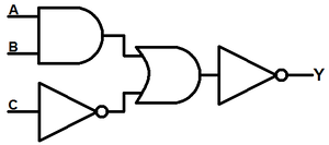
Implement the Verilog description of the module with the inputs a, b, c and the output y, with the functionality in the diagram below. Implement the circuit on the DE1/De1-SoC board by connecting inputs a, b, c to SW5, SW6, and SW7 respectively, and output y to LEDR4.
Exercise 6
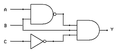
Implement the Verilog description of the module with the inputs a, b, c and the output y, with the functionality in the diagram below. Implement the circuit on the DE1/De1-SoC board by connecting inputs a, b, c to SW5, SW4, and SW1, and output y to LEDR7.
Submission of Exercise Solving
It will solve a single exercise, which will be selected by the teacher. For scoring, the following files will be submitted to the e-mail address indicated by the teacher.
An archive zip
- A Verilog file with the .v extension that contains the Verilog description of the circuit
- A constraint file with the .qsf extension
- A Quartus project file with the .qpf extension
Note that the archive will contain only the 3 files (no directories).
The subject of the email message must follow the [Name] _ [First Name] _ [Group] _ [Exercise Number] For example Petrica_Lucian_423B_2
Recommendations for Teachers
- Implementing a Quartus project example, going through the tutorial.
