Diferență între revizuiri ale paginii „Introduction to FPGA synthesis. Xilinx ISE.”
Cbira (discuție | contribuții) |
Cbira (discuție | contribuții) |
||
| Linia 70: | Linia 70: | ||
* [[Spartan 3 Starter Board]] | * [[Spartan 3 Starter Board]] | ||
* [[Nexys 2]] | * [[Nexys 2]] | ||
| + | * [[DE1 | https://www.altera.com/solutions/partners/partner-profile/terasic-inc-/board/altera-de1-board.html]] | ||
| + | * [[DE1-SoC | https://www.altera.com/solutions/partners/partner-profile/terasic-inc-/board/altera-de1-board.html]] | ||
For all available plates, the model code as the package code is written directly on the chip. | For all available plates, the model code as the package code is written directly on the chip. | ||
Versiunea de la data 30 mai 2018 09:08
FPGA (Field Programmable Gate Array)
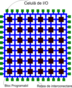
The Field Programmable Gate Array (FPGA) is a generic circuit that can be programmed to implement any user-defined function. An FPGA consists of a programmable block matrix, an interconnection network linking these blocks together, I / O circuits and a SRAM memory that configures these structures. The figure below presents a simplified FPGA schematic.
Programmable blocks can be generating logic functions, RAM memories, or propagation circuits. The figure shows the structure of a logic function generator block. This consists of a Look-Up Table (LUT) and a register to synchronize its output if desired. A LUT can implement any logical function of 4 variables with using a selector. Each combination of input variable values selects the corresponding result, pre-calculated by the synthesis program and stored in the configuration memory when programming the FPGA. The output of the logic function generator can be linked either to the register or directly to the LUT output.
Each programmable block is linked to the interconnection network. It consists of programmable threads and switches. Each switch can couple two or more segments together, as can be seen in the figure. Switch status (on / off) is also predetermined in the Place and Route stage, and stored in the configuration memory.
Steps of synthesis
When programming a FPGA with a new circuit, it follows a series of procedures that transform it from hardware description code (Verilog, VHDL, etc.) into a bit string that configures the chip. These steps are:
- Synthesis - is the stage where the Verilog code is interpreted by the synthesis program that generates from it a circuit (the assembly of gates and registers) named netlist ; this stage is independent of the FPGA model with which it is working;
- Implementation - the step at which the gateway circuit (netlist) is translated into the element level circuit available on the FPGA chip used; This step obviously depends on the FPGA model used;
- Programming file generation - From the previous point circuit, a file with the extension .bit is generated which contains the configuration bit for the logic blocks, the I / O blocks and the interconnection blocks corresponding to the desired circuit;
- Device programming - the stage where, through a JTAG interface, the file .bit is loaded into the FAMA's SRAM memory, thus configuring the device.
Warning: Test modules are NOT used in for synthesis! Therefore, a test module should not appear in Xilinx, but only in Modelsim!
Configuring the I / O
External Links
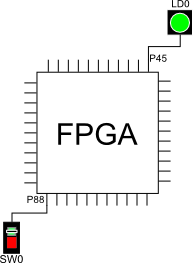
I / O devices (input - output) are connected to the outside of the FPGA chip to one pin. Each of these pins has a known name of the synthesis program. These names differ from one FPGA model to another. In the figure given as an example, a switch (SW0) that is an input device is connected to the pin named "P88" of the FPGA and a led (LD0) is connected to the pin "P45", which is a output device. These bindings are physically made to produce plates and can not be modified. Therefore, most of the time, in each of the devices on a development board, the index or the name of the FPGA pin to which it is linked is in brackets.
For the Pegasus development board, the pin index is passed to each device. For example, next to the switch SW0 is the number (89) in parentheses. In this case, the full name of the pin when making the internal links in the FPGA is P89. Analog for all devices on the board.
For the Spartan-3 Starter Board FPGA development board, the name of the pin is passed next to each device. For example, next to the switch SW0 is passed in parentheses (F12), which is even the name of the pin. Analog for all devices on the board.
Internal Links
Internal links are the logical connections between each bit of the main module ports and the FPGA pins. These links make it possible to connect external devices on the development board to user-defined Verilog mode. For example, if the FPGA board is configured with a 4-bit sumer, then we want each bit of the input ports to be connected to one switch, and each bit of the output port is linked to one led, or other output device. These links are not permanent, so at each plate configuration these links must be specified in the synthesis program before the implementation step. The link specification is given in a file called Implementation Constraints File , which must be added to the ISE project, and has the following syntax:
net "in0 [0]" loc = "P88";
This line expresses the fact that bit 0 (the least significant) of port in0 (which in the Adder module is an input) is internally linked to pin P88 Pegasus is further tied to the SW0 switch.
Note: Analogue to Verilog, if the port has one bit, its index is missing:
net "port_de_un_bit" loc = "P88";
Rule: For each bit of each port of the main module, a line must appear in the constraint file where it is linked to the desired device on the board.
Entries in Verilog are defined with the word input , outputs are output. Any module starts with the word modules and ends with endmodule . Modules can not overlap and can not be included in each other.
Xilinx ISE
The program used in the laboratory for circuit synthesis is ISE Design Suite, from Xilinx. You have the 4-bit summation synthesis tutorial on the [[Xilinx ISE Tutorial] page.
Available FPGA boards
In the CID lab you can work with one of the following development boards:
- Pegasus
- Spartan 3 Starter Board
- Nexys 2
- https://www.altera.com/solutions/partners/partner-profile/terasic-inc-/board/altera-de1-board.html
- https://www.altera.com/solutions/partners/partner-profile/terasic-inc-/board/altera-de1-board.html
For all available plates, the model code as the package code is written directly on the chip.


