Diferență între revizuiri ale paginii „Applications 3”
| Linia 164: | Linia 164: | ||
Recompile the design file (from the simulator), and restart simulation. | Recompile the design file (from the simulator), and restart simulation. | ||
| − | Implement the design using 2 buttons (BTN0 and BTN1 ) for the inputs in0 and in1, one switch (SW0) for selection, and one LED (LED0) for the multiplexer output (c). | + | Implement the design using 2 buttons (BTN0 and BTN1 ) for the inputs in0 and in1, one switch (SW0) for selection, and one LED (LED0) for the multiplexer output (c): |
| + | |||
| + | [[Fișier: Dic_lab3_mux_fpga.png]] | ||
| + | |||
| + | The constraints file sets the connections between the mux ports and the FPGA pins. | ||
| + | Taking the first constraint as an example, fill in the missing port names for the next three constraints: | ||
| + | |||
| + | <syntaxhighlight> | ||
| + | ##Switches | ||
| + | set_property -dict { PACKAGE_PIN M20 IOSTANDARD LVCMOS33 } [get_ports { s }]; #SW 0 | ||
| + | |||
| + | ##Buttons | ||
| + | set_property -dict { PACKAGE_PIN D19 IOSTANDARD LVCMOS33 } [get_ports { }]; #BTN 0 | ||
| + | set_property -dict { PACKAGE_PIN D20 IOSTANDARD LVCMOS33 } [get_ports { }]; #BTN 1 | ||
| + | |||
| + | ##LEDs | ||
| + | set_property -dict { PACKAGE_PIN R14 IOSTANDARD LVCMOS33 } [get_ports { }]; #LED 0 | ||
| + | </syntaxhighlight> | ||
== Exercise 5 == | == Exercise 5 == | ||
Versiunea de la data 13 martie 2022 23:50
Behavioral descriptions, continuous assignment, conditional instructions, use of blocks always for describing combinational circuits.
Structural descriptions, logic gates, verilog gate primitives.
Exhaustive verification. Loop statements in testbenches.
Exercise 1
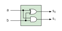
half adder - gate-level description
The half-adder is the simplest, 1-bit, adder. It implements the addition of two bits.
| a | b | c |
|---|---|---|
| 0 | 0 | 0 0 |
| 0 | 1 | 0 1 |
| 1 | 0 | 0 1 |
| 1 | 1 | 1 0 |
Use data flow description (a simpler kind of behavioral description that uses logic expressions). Logic expressions employ only logic operators.
| operator | function |
|---|---|
| ~ | not |
| & | and |
| | | or |
| ^ | xor |
One assign instruction for each output. Concurrent assignments (in simulation they are evaluated in parallel, mimicking the parallelism of the real circuits)
assign c[0] = a ^ b;
assign c[1] = a & b;
Bit selection operator ([ ]) is used to select a bit (or a couple of consecutive bits) from a multibit variable.
If c is declared as a 2 bit output, each of its bits may be separately controlled. The index must be a positive integer in the range set when the variable was declared.
If myVariable was declared of type output [7:0], then the integer used for selection must not exceed 7.
repeat statement in testbenches
An exahaustive test is a test that generates all possible combinations of values for the inputs of the dut. Write a testbench for the half-adder that uses a repeat statement to generate all input combinations, and a concatenation operator that makes possible to update two or more variables at the same time.
initial begin
    {a, b} = 0;
    repeat (4) #1 {a, b} = {a, b} + 1;
end
Some remarks:
- There is no increment operator in verilog.
- Adding 1 to 3 on 2 bits turns around to 0.
- A delay may precede a statement.
Exercise 2
1-bit half adder - structural description
Work on the same project as that of Exercise 1. You need only to modify the description of the half-adder module.
Gate-level description = a structural description that uses only logic gates.
Verilog gate primitives: not, and, nand, or, nor, xor and xnor. Except for the not gate, all other primitive gates may have 2, 3 or more inputs.
All gate primitives are instantiated using the same template: gatePrimitiveType myGate(outputConnection, inputConnection1, inputConnection2 ...) as in the following examples:
not g1(dout, din); is a not gate with dout at output and din connected at its input.
nand g2(dout, d1, d2); is a nand gate with dout at output and two wires, d1 and d2, connected to its inputs.
nand g3(dout, d1, d2, d3, d4); is a nand gate with dout at output and four inputs, connected to d1, d2, d3 and d4.
Using gate primitives, a possible structural description of the half-adder may be:
xor g1(c[0], a, b);
and g2(c[1], a, b);
Recompile the design file (from the simulator), and restart simulation.
Implement the design using 2 switches (SW0 and SW1) as inputs a and b, and two LEDs (LED0 and LED1) to show the result, c.
Exercise 3
2 to 1 multiplexer, behavioral description
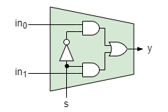
The simplest selection logic circuit. It selects between two inputs, in0 and in1, based on the value of the selection input, s:
| s | c |
|---|---|
| 0 | in0 |
| 1 | in1 |
always block. Used for behavioral descriptions. Template:
always @(sensitivity list) begin
block of instructions
end
For combinational circuits the safest way to declare the sensitivity list is to use the wildcard (*). It stands for all variables that appear on RHS expressions and in evaluation expressions.
always @(*) begin
  if(s)
    c = in[1];
  else
    c = in[0];
end
Any variable that gets value through assignments inside an always block must be declared of type reg.
If the variable is also an output of the module, the output is declared as output reg.
for statement in testbenches
Write a testbench using a for statement to generate all input combinations. Its template is:
for(initial_assignment; expression; step_assignment) block of statements;
The foor loop is repeated until the expression evaluates true. The simplest for statement uses an integer index that is incremented at the end of each iteration. The for loop below generates all combinations from 000 to 111 for tree logic variables, s, a and b. The index must be declared as a variable of type integer.
initial begin
    {s, a, b} = 0;
    for(index = 0; index < 8; index = index + 1) begin
        #1 {s, a, b} = {s, a, b} + 1;
    end
end
Exercise 4
2 to 1 multiplexer - gate-level description
Work on the same project as that of Exercise 3. You need only to modify the description of the 2 to 1 multiplexer module.
Implement the 2 to 1 multiplexer using only verilog gate primitives. For simulation you may reuse the testbench from Exercise 3 (copy its file into the directory of this project and set it as the testbench). Change the type of the multiplexer's instance in the testbench, if it is different from Exercise 3.
Recompile the design file (from the simulator), and restart simulation.
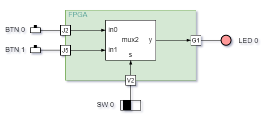
Implement the design using 2 buttons (BTN0 and BTN1 ) for the inputs in0 and in1, one switch (SW0) for selection, and one LED (LED0) for the multiplexer output (c):
The constraints file sets the connections between the mux ports and the FPGA pins. Taking the first constraint as an example, fill in the missing port names for the next three constraints:
##Switches
set_property -dict { PACKAGE_PIN M20   IOSTANDARD LVCMOS33 } [get_ports { s }]; #SW 0

##Buttons
set_property -dict { PACKAGE_PIN D19   IOSTANDARD LVCMOS33 } [get_ports { }]; #BTN 0
set_property -dict { PACKAGE_PIN D20   IOSTANDARD LVCMOS33 } [get_ports { }]; #BTN 1

##LEDs
set_property -dict { PACKAGE_PIN R14   IOSTANDARD LVCMOS33 } [get_ports { }]; #LED 0
Exercise 5
4 to 1 multiplexer - behavioral description
case instruction. Selects between multiple cases. Template
case(selectVariable)
value1 : instruction block 1
value2 : instruction block 2
a.s.o.
endcase
value1, value2 a.s.o. are integer values of the selectVariable
case(s)
  0: c = in[0];
  1: c = in[1];
  2: c = in[2];
  3: c = in[3];
endcase
Exercise 6
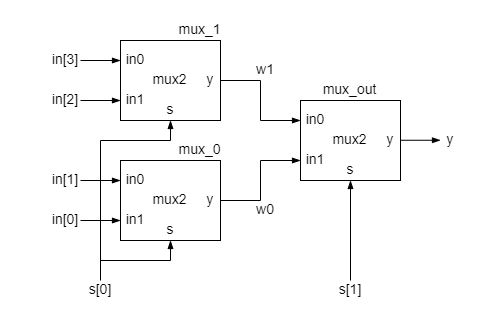
4 to 1 multiplexer - structural description
Implement the 4 to 1 multiplexer using three instances of the 2 to 1 multiplexer (add to the project the file of that module either from Exercise 3, or Exercise 4) and a primitive gate.
Be careful to distinctly name each instance and each internal wire!


