Diferență între revizuiri ale paginii „CID Seminar EN”
Cbira (discuție | contribuții) (Pagină nouă: In this seminar you will learn what is a secession circuit and how it is described in Verilog. '''Keywords:''clock'',''flip-flop'', blocking''/''non-blocking' Verilog syntax: ''a...) |
Cbira (discuție | contribuții) |
||
| Linia 14: | Linia 14: | ||
* synchronous reset signal with the clock, active on the 0 scale | * synchronous reset signal with the clock, active on the 0 scale | ||
| − | <u> Additional explanation </ u> | + | <u> Additional explanation </u> |
The most commonly used circuit to synchronize any clock signal is the flip-flop D (also called flip-flop FF). The binary D in this example has the following ports: | The most commonly used circuit to synchronize any clock signal is the flip-flop D (also called flip-flop FF). The binary D in this example has the following ports: | ||
| Linia 30: | Linia 30: | ||
In clock processes, signal values are assigned using the non-blocking assignment (with the operator <=, which in this context means "takes the value", and NOT less than or equal !!!) unlike the processes' '' always' '' that describe purely combinational circuits and where assigning new values is done using only the blocking assignment (with operator =). | In clock processes, signal values are assigned using the non-blocking assignment (with the operator <=, which in this context means "takes the value", and NOT less than or equal !!!) unlike the processes' '' always' '' that describe purely combinational circuits and where assigning new values is done using only the blocking assignment (with operator =). | ||
| − | </ | + | </div> |
== Exercise 2 == | == Exercise 2 == | ||
| Linia 36: | Linia 36: | ||
Simulate the operation of the bistable D. At the CK input a periodic signal with a period of 6 time units will be applied. | Simulate the operation of the bistable D. At the CK input a periodic signal with a period of 6 time units will be applied. | ||
| − | <u> Additional explanation </ u> | + | <u> Additional explanation </u> |
The clock signal has the following properties: | The clock signal has the following properties: | ||
| Linia 51: | Linia 51: | ||
[[File: sem3_ex1.png | Figure 1 - Combined Logic Circuit (CLC)]] | [[File: sem3_ex1.png | Figure 1 - Combined Logic Circuit (CLC)]] | ||
| − | <u> Additional explanation </ u> | + | <u> Additional explanation </u> |
<div class = "rule"> | <div class = "rule"> | ||
| Linia 57: | Linia 57: | ||
When using '''always'''the signal must be declared. | When using '''always'''the signal must be declared. | ||
| − | </ | + | </div> |
The hazard (behavior of combinational circuits that is not in accordance with logical algebra) is due to propagation times through logical gates. To highlight this phenomenon, we will introduce the propagation times through gates with the syntax: | The hazard (behavior of combinational circuits that is not in accordance with logical algebra) is due to propagation times through logical gates. To highlight this phenomenon, we will introduce the propagation times through gates with the syntax: | ||
| Linia 68: | Linia 68: | ||
[[File: sem3_ex5.png | Figure 3 - A Sequential Circuit]] | [[File: sem3_ex5.png | Figure 3 - A Sequential Circuit]] | ||
| − | <u> Additional explanation </ u> | + | <u> Additional explanation </u> |
The circuit can be described in two ways: | The circuit can be described in two ways: | ||
* separating the combined side from the sequential (using 2 processes '''always''') | * separating the combined side from the sequential (using 2 processes '''always''') | ||
| − | * using a single process '' 'always' '' | + | * using a single process '''always''' |
The simulation will highlight the elimination of the hazard on the output. | The simulation will highlight the elimination of the hazard on the output. | ||
| Linia 107: | Linia 107: | ||
'''Note''': This example will help you understand the above rule: Always use the non-blocking assignment''' <= ''' to describe synchronous clock circuits. | '''Note''': This example will help you understand the above rule: Always use the non-blocking assignment''' <= ''' to describe synchronous clock circuits. | ||
| − | <u> Additional explanations </ u> | + | <u> Additional explanations </u> |
The difference between the blocking and the non-blocking assignment types is as follows: unlike the blocking assignment (=), the non-blocking assignment (<=) does not immediately update the left regression signal, but only the end of the pa | The difference between the blocking and the non-blocking assignment types is as follows: unlike the blocking assignment (=), the non-blocking assignment (<=) does not immediately update the left regression signal, but only the end of the pa | ||
Versiunea de la data 5 aprilie 2018 08:20
In this seminar you will learn what is a secession circuit and how it is described in Verilog.
Keywords:clock,flip-flop, blocking/non-blocking'
Verilog syntax: always, initial, forever
The digital circuits are of two types:
- Combinational logic circuits (CLC) - can be described either using 'assign' or using '
- sequential circuits - can be described using only always
Exercise 1
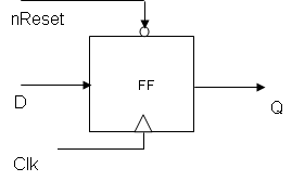
Describe in Verilog a bistable D with the following features:
- active clock signal on the positive front
- synchronous reset signal with the clock, active on the 0 scale
Additional explanation
The most commonly used circuit to synchronize any clock signal is the flip-flop D (also called flip-flop FF). The binary D in this example has the following ports:
- Clk - clock input, active on the positive front
- D - Data entry
- nReset - synchronous clock signal input; nRest active on the 0 field
- Q - circuit output
Remark: The reset signal will always be synchronous with the clock, ie it will change its value from 1 to 0 or vice versa always on the active front of the clock !!!
The description of a RTL verilog in Verilog is only possible using always-type processes, with the sensitivity list at least the positive clock face.
In clock processes, signal values are assigned using the non-blocking assignment (with the operator <=, which in this context means "takes the value", and NOT less than or equal !!!) unlike the processes' always' that describe purely combinational circuits and where assigning new values is done using only the blocking assignment (with operator =).
Exercise 2
Simulate the operation of the bistable D. At the CK input a periodic signal with a period of 6 time units will be applied.
Additional explanation
The clock signal has the following properties:
- Rectangular signal (like all other digital signals)
- It's a regular signal
- It's the only signal in a digital system that's active on the front. All other signals present in a digital system are active on the floor.
Exercise 3
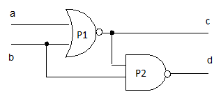
The combination circuit in the following figure has a hazard on the output. Describe this circuit in Verilog using a 'assign' statement and an 'always' process and then simulate its operation to highlight the hazard.
Additional explanation
When you use assign - the signal must be declared 'wire' '.
When using alwaysthe signal must be declared.
The hazard (behavior of combinational circuits that is not in accordance with logical algebra) is due to propagation times through logical gates. To highlight this phenomenon, we will introduce the propagation times through gates with the syntax: assign #tp ..., where tp is the propagation time.
Exercise 4
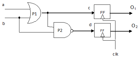
Describe the circuit in the following figure in Verilog and simulate its operation.
Additional explanation
The circuit can be described in two ways:
- separating the combined side from the sequential (using 2 processes always)
- using a single process always
The simulation will highlight the elimination of the hazard on the output.
Exercise 5
Simulate and compare the operation of the following circuits (in the two modules only the type of assignment used: non-blocking or blocking):
Circuit 1:
always @ (posedge clk) begin
    if (nReset == 0) begin
        b <= 0;
        c <= 0;
    end else begin
        b <= a;
        c <= b;
    end
end
Circuit 2:
always @ (posedge clk) begin
    if (nReset == 0) begin
        b = 0;
        c = 0;
    end else begin
        b = a;
        c = b;
    end
end
Note: This example will help you understand the above rule: Always use the non-blocking assignment <= to describe synchronous clock circuits.
Additional explanations
The difference between the blocking and the non-blocking assignment types is as follows: unlike the blocking assignment (=), the non-blocking assignment (<=) does not immediately update the left regression signal, but only the end of the pa


