Xilinx Platform Studio
Xilinx Platform Studio enables its user to easily build hardware platforms based on the Microblaze soft processor and various development boards from Xilinx and other vendors. XPS is part of the Xilinx Embedded Development Kit (EDK), which itself is part of the Xilinx ISE Embedded and System Editions. For this tutorial, ISE 14.2 System Edition was used. The tutorial shows how to create a simple hardware system for the Digilent Nexys 2 board.
Getting Started
Start the Platform Studio, which will show a welcome menu with icons laid out in two columns: Getting Started and Documentation. From the Getting Started column, select the first option, Create New Project Using Base System Builder. This will start a wizard which will help the user configure and generate a hardware system.
Base System Builder
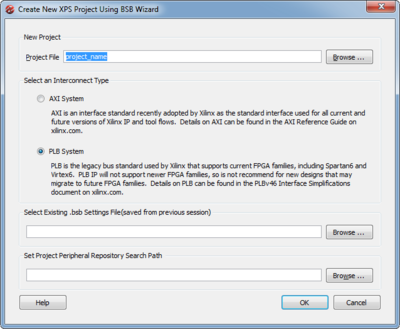
In the first window of the wizard, enter the name of your project. We will be using the project name xps_tutorial for the duration of this tutorial.
Next, select the interconnect type. AXI interconnects are generally used with ARM processors or newer FPGAs. Since we will be using a Microblaze processor on a Spartan-3 FPGA, select PLB and click OK.
In the Welcome window, select I would like to create a new design and click Next.
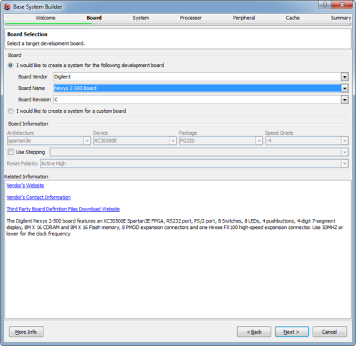
In the Board window, choose from the drop-down menus to build a system for the Nexys 2-500 board from Digilent. Information about the board, as well as links to the manufacturer, are available in the lower part of the wizard window.
In the System window, select to create a single-processor system.
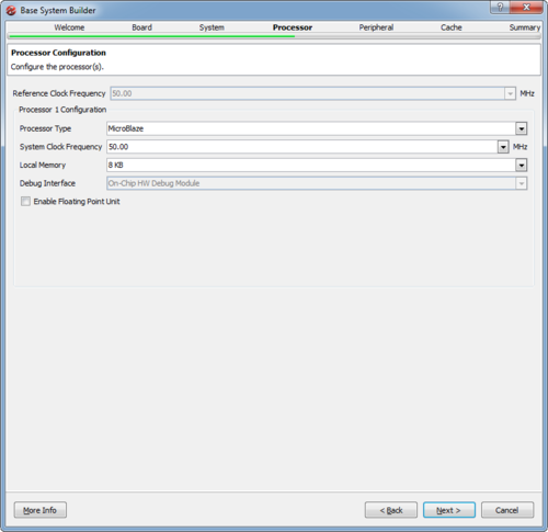
In the Processor window, select the Microblaze processor and 50 Mhz from the frequency drop-down menu. Change the Local Memory selection to 16KB or more from the default 8KB if you intend to implement more complex software projects on the hardware platform. Also, the user may choose to add hardware floating-point support to the Microblaze processor. For this tutorial, the local memory will be set at 8KB, and hardware floating-point will be disabled.
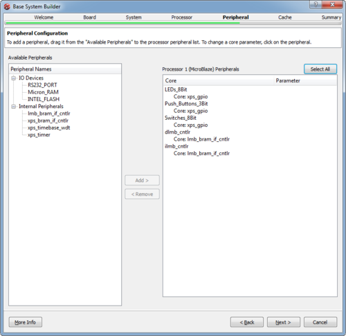
In the Peripheral window, remove the RS232_PORT, Micron_RAM and INTEL_FLASH peripherals. Notice that in the right panel the peripherals can be selected and certain parameters may be modified by the user.
In the Cache window, click Next since there is no cacheable memory to configure in the system.
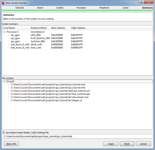
In the Summary window, the wizard will display a summary of the configured system, including processors, peripheral names and their system addresses. Project file names are also shown along with their complete system paths. Click Finish when you are done reviewing your system configuration.
The wizard will now proceed to generate all project files and load the project into the Platform Studio user interface.
Platform Studio GUI
The graphical user interface of Xilinx Platform Studio is split into three main panels. To the left there is the Navigator panel. Top-right and center are the System Assembly panel and the IP Catalog respectively. The bottom panel is the console window, along with warning and error tabs.
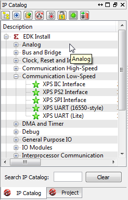
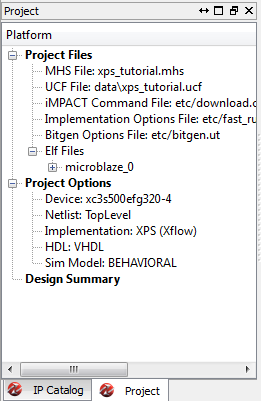
The IP Catalog is a database of pre-designed peripherals and accelerator cores supplied by Xilinx as part of the ISE System Edition software package. Right-clicking on any item in the catalog will enable the user to add the item to the hardware system. The new system will need to be connected and mapped in the address space of the processor. Co-located with the IP Catalog is the Project tab, which shows information on file location, target FPGA and other project properties.
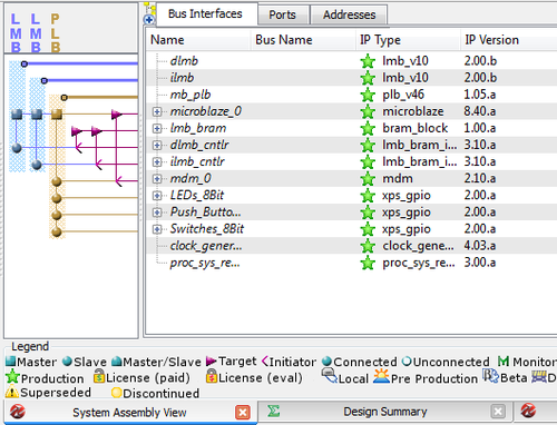
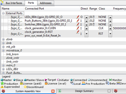
The System Assembly panel contains three tabs: Bus Interfaces, Ports and Addresses.
The Bus Interfaces tab allows components to be connected and disconnected from system busses and the bus layout to be viewed in graphical form.
The Ports tab allows connection of IO signals between components and FPGA pins, but can also be used to connect components with each-other or to connect global signals like clock and reset to individual system components.
The Addresses tab shows the processor address map split into regions corresponding to each peripheral. The amount of memory allocated to each peripheral is configurable. Peripheral address spaces can also be locked.
Generating Peripherals
XPS allows the user to generate custom peripherals. In order to do this, go to Hardware -> Create or Import Peripheral, which will start the peripheral creation wizard.
In the first welcome screen, click Next. In the next window, select Create templates for a new peripheral, then click Next.
In the Repository or Project window, select to store the peripheral to an XPS project. The default setting is to store the peripheral to the project which was open when the wizard was started in XPS.
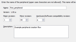
In the Name and Version window, give your peripheral a name, a version number and a description. In this example we will use the name first_peripheral and the default version number
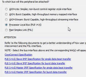
The following window allows the user to select which type of bus the peripheral will use for its connection to the system processor. Select PLB to generate a peripheral which is compatible with the example XPS project used in this tutorial. The lower part of the wizard window shows links to relevant documentation about the selected bus.
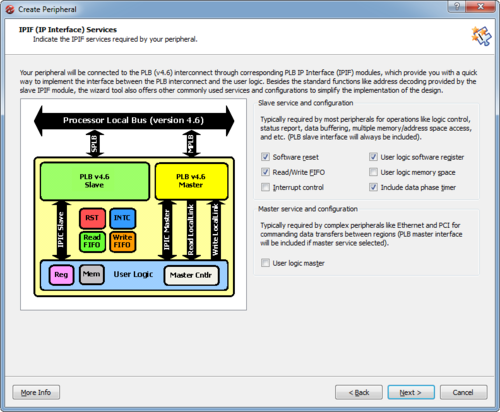
The IPIF Services window allows the user to configure the interface of the peripheral with the bus. The user can enable the generation of various interface circuitry. Enable the software register, the read/write FIFOs, the user logic software register and the data phase timer.
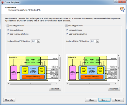
In the Slave Interface window, just click Next. The following window configures the FIFO Service. Because we have selected to add read/write FIFOs to the bus interface, we can configure the parameters of these FIFOs. Deselect Packet Mode for both the Write FIFO and the Read FIFO. Please note that Read and Write is from the perspective of the system processor. Detailed information about the FIFO circuitry can be accessed by clicking on the Datasheet button corresponding to each FIFO.
The User SW Register window allows the user to select the number of software-accesible registers generated. Specify to select 8 registers, and click Next. Do the same in the following two windows, which will bring you to the Peripheral Implementation Support window. Enable Generate stub user_logic template in Verilog instead of VHDL. Click OK in the resulting warning pop-up window. Click Next to go to the final wizard screen.
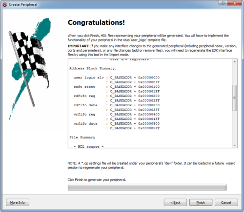
In the Congradulations window you are shown the final settings for the configured peripheral. Please note the generated address space, which shows offsets from the peripheral base address for software registers, the reset register and the fifo interfaces.
Click Finish to generate your peripheral. It will be stored in the project folder, under the subfolder pcores/first_peripheral. Under first_peripheral/hdl/verilog you will find a Verilog file called user_logic.v which contains example logic for the software register interface, and all signals required to work with the FIFO interfaces.
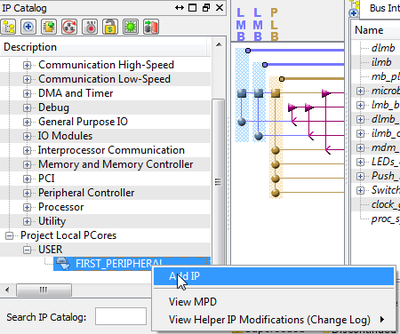
Following the generation, your peripheral will be available in XPS in the IP Catalog window, under Project Local PCores.
Adding Peripherals to the System
We will now integrate the peripheral generated in the previous section to our system. The first step is to look for the peripheral in the IP Catalog and add it to the peripheral list. Select Add IP from the right-click menu and click OK in the pop-up window which follows.
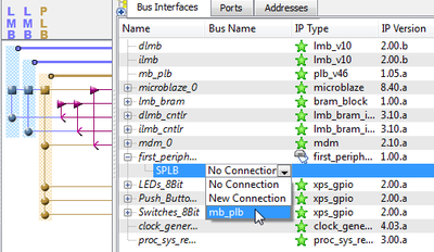
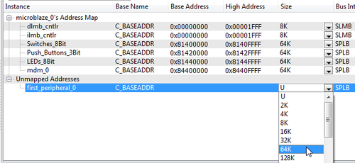
Next, we must connect the peripheral to the PLB bus by selecting mb_plb in the bus drop-down menu. This will connect the peripheral to the main PLB bus and add an unmapped address space in the Addresses tab. From Addresses select 64KB as the memory space size.
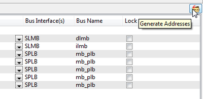
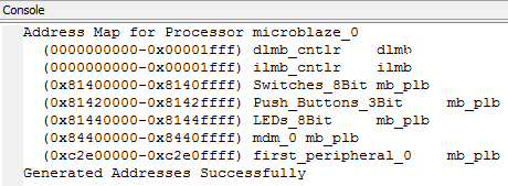
Next, click on Generate Addresses in the top-right corner in order for the system address map to be recalculated. If successful, the Console window will show the new address map, and the Addresses tab will also be updated with the new address map.
Exporting to SDK
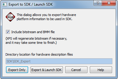
In the Navigator panel, notice the Export to SDK option. After the project is configured and you have generated a bitfile, click this button to export the project to Xilinx SDK. A pop-up window will appear with the following contents:
Select to export the bitfile along with the project, and click on Export & Launch SDK. This will process the project into a form which is understandable by SDK and will then launch SDK with your hardware project loaded, and ready to create software applications.
