Applications 5
Description
Design and verify a decimal adder with 2 digit input numbers.
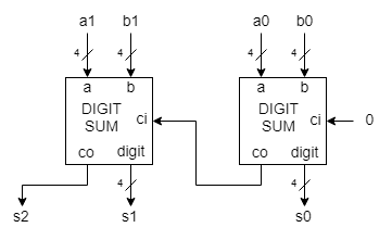
The top level design (Figure 1) has 2 blocks, of type digitsum, each block adding digits of the same range.
Figure 1 .
(Top level design)
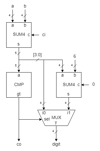
The digitsum block (Figure 2) comprises 4 subblocks, two 4 bit binary adders, instances of sum4, one instance of cmp and a simple 2 to 1 multiplexer.
Figure 2.
( the DIGIT SUM block )
The first adder adds the 4 bit inputs, giving a binary result in the range [0 ... 18].
The comparator, cmp, outputs 1 if the result is greater than 9.
If the result is not greater than 9, than it is sent out directly to the digit output of the digitsum block (the result MSB is thrown away).
If the result is greater than 9, a correction must be made, adding 6 to the result.
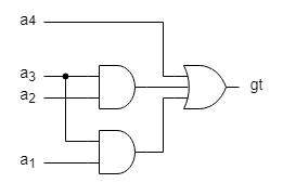
The comparator with 9, cmp, is described at the gate level:
Figure 3
Testbench
The testbench must generate stimuli for bcdsum as in Figure 4.
b0 input of bcdsum changes at each 5 simulation steps.
b1, a0 and a1 change synchronously with b0 as in figure 4.
Figure 4
Requirements
- cmp module is described structurally at the gate level as in Figure 3.
- sum4 module is described behaviorally with a continuous assignment.
- mux module is described behaviorally within an always process.
- digitsum module is described structurally as in Figure 2. It has 4 instances of the proper type.
- the top-level design module, bcdsum, is described structurally as in Figure 1.
- write the testbench module, bcdsum_tb, that instantiates the top-level module bcdsum with the instance name dut.
- in the testbench, generate stimuli for the dut inputs.
- in the wave panel of the simulation change the radix to unsigned decimal and zoom full.
Interfaces
cmp(a, gt)
mux(y, sel, i1, i0)
sum4(a, b, c, s)
digitsum(a, b, ci, co, digit)
bcdsum(a1, a0, b1, b0, s2, s1, s0)
bcdsum_tb // the testbench module has no pins


