DIC Lab Work 1
Notions and Knowledge Required
- Using the Altera Quartus II Synthesis Program
- List of pins for plate DE1
- Plate pin list DE1_SOC
- Boolean Logic and Numerical Systems
- Syntax notions Verilog
Example
Create a new project in Quartus II for the Altera Cyclone II FPGA on the DE1 board. Create a Verilog source file within the project, and copy the next module to the file.
Warning! The name of the top-level module to be synthesized should be set correctly when you create the project (in this case, OrGate).
<syntaxhighlight lang="Verilog"> OrGate modules ( output out, input in1, input in2 )
assign out=in1 | in 2;
endmodule <syntaxhighlight>
Add the necessary constraints for the circuit's inputs and outputs to be connected as follows:
- in1 connected to SW0: PIN_L22
- in2 connected to SW7: PIN_M2
- Out connected to LDR3 (red LED no.3): PIN_Y19
Implement the project on the DE1 board and observe the circuit functionality described by the Quartus II project.
The list of pins to which I /O devices are connected to the DE1 board are described here
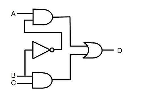
Exercise 1
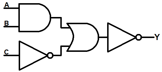
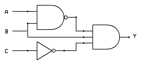
Make the Verilog description of the module with the inputs a, b, c and the output d with the functionality shown in the diagram below. Implement the circuit on the DE1 board by connecting inputs a, b, c to SW2, SW4, and SW6 respectively, and output d to LEDG2.
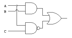
Exercise 2
Make the verilog description of the module with the inputs a, b, c and the output q with the functionality in the diagram below. Implement the circuit on the DE1 board by connecting inputs a, b, c to SW3, SW4, and SW7, and output q to LEDR7.
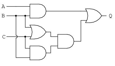
Exercise 3
Make the verilog description of the module with the inputs a, b, c and the output q with the functionality in the diagram below. Implement the circuit on the DE1 board by connecting inputs a, b, c to SW1, SW6, and SW7, and output q to LEDG3.
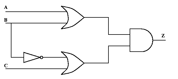
Exercise 4
Make the description in Verilog of the module with the inputs a, b, c and the output z with the functionality in the diagram below. Implement the circuit on the DE1 board by connecting inputs a, b, c to SW3, SW4, and SW5, and output z to LEDR6.
Exercise 5
Make the Verilog description of the module with the inputs a, b, c and the output y, with the functionality in the diagram below. Implement the circuit on the DE1 board by connecting inputs a, b, c to SW5, SW6, and SW7 respectively, and output y to LEDG4.
Exercise 6
Make the Verilog description of the module with the inputs a, b, c and the output y, with the functionality in the diagram below. Implement the circuit on the DE1 board by connecting inputs a, b, c to SW5, SW4, and SW1, and output y to LEDR7.
Submission of Exercise Solving
It will solve a single exercise, which will be selected by the teacher. For scoring, the following files will be submitted to the e-mail address indicated by the teacher.
An archive zip
- A Verilog file with the .v extension that contains the Verilog description of the circuit
- A constraint file with the .qsf extension
- A Quartus project file with the .qpf extension
Note that the archive will contain only the 3 files (no directories).
The subject of the email message must follow the [Name] _ [First Name] _ [Group] _ [Exercise Number] For example Petrica_Lucian_423B_2
Recommendations for Teachers
- Implementing a Quartus project example, going through the tutorial.
