Applications 6
Exercise 1
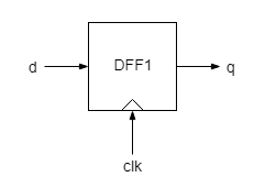
D flip-flop
- dff module with behavioral description of the D flip-flop
- dff_tb testbench with stimuli for d and clk
the output takes the value of the input, q <= d, but only at discrete moments of time,
when the control signal clk changes from 0 to 1, always @(posedge clk).
Attention!
- behavioral sequential descriptions use only always processes
- any sequential variable is of reg type
- all assignments for sequential variables are nonblocking assignments, i.e. they use the
<=operator
clock generation in testbench
initial begin
    clk = 0;                // initialization at time 0
    forever #10 clk = ~clk;  // toggle the clock at each 10 simulation steps
end
For the d input generate the following sequence in testbench:
See how the output q reacts or not to changes of the input d.
Exercise 2
4 bit D register
- reg4 module
- reg4_tb testbench with stimuli for d and clk
The behavioral description is identical with that of the D flip-flop of Exercise 1 (the D flip-flop being nothing else than a 1 bit D register). However, the interface differs in terms of the widths for d input and q output.
For the d input generate the following sequence in testbench:
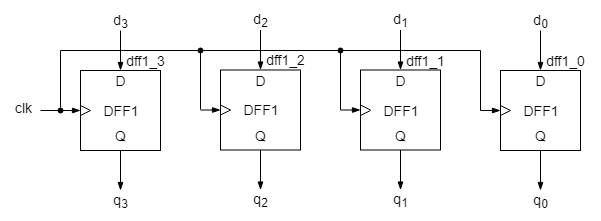
structural description with flip-flops
- add dff file to this project
- change the description of reg4 to a structural one, with 4 instances of dff, connected as in the schematics below:
- rerun the testbench
Exercise 3
4 bit shift left register
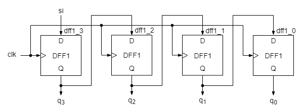
- shiftr4 module described structurally as in the schematics below. It is basically the reg4 module, but with the D flip-flops connected in a shift chain.
- dff is added (copied) to this project
- shiftr4_tb testbench with clk generation and a (random) bit sequence for si (serial input)
reset
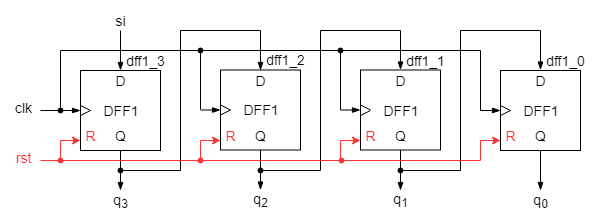
Almost always a sequential circuit needs to start from a valid configuration, usually the initial one (for example with all bits zero). Without a proper reset the shift register will start in a random configuration, and its outputs will be meaningless untill the first input bit is shifted till the rightmost position, which takes 4 clock cycles. In simulation the outputs will be undefined until the first input bit reaches them.
The reset is active for a short time after power up (at the beginning of the simulation). The active value may be 1 or 0.
Also, the reset may be synchronous or asynchronous. The synchronous reset takes effect only at the first active clock edge after the reset is applied (therefore, the syncronous reset pulse must last at least one clock cycle). The asynchronous reset has immediate effect.
For any sequential process with reset (active 1 in the examples below) the template is:
- for synchronous reset
always @(posedge clk) begin
    if(rst) begin
        // initialize sequential variables
    end
    else begin
        // sequential variables normal control
    end
end
- for asynchronous reset
always @(posedge clk, posedge rst) begin
    if(rst) begin
        // initialize sequential variables
    end
    else begin
        // sequential variables normal control
    end
end
behavioral description
- change the shiftr4 to a behavioral one. Use a single always process to control each output bit
- check in testbench that the behavior is correct
nonblocking versus blocking assignments
- compare in simulation these two behavioral descriptions of the shiftr4 module:
    q[3] <= si
    q[2] <= q[3]
    q[1] <= q[2]
    q[0] <= q[1]
    q[3]  = si
    q[2]  = q[3]
    q[1]  = q[2]
    q[0]  = q[1]


