Applications 11: Diferență între versiuni
(Pagină nouă: == Requirement == ''Design, verify and implement a calculator. It adds, subtracts or multiplies an 8 bit number to/from the current content of its accumulator. It continuously disp...) |
|||
| Linia 9: | Linia 9: | ||
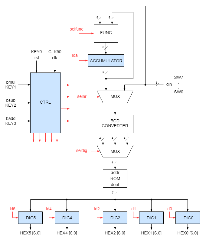
[[Fișier: calc.png]] | [[Fișier: calc.png]] | ||
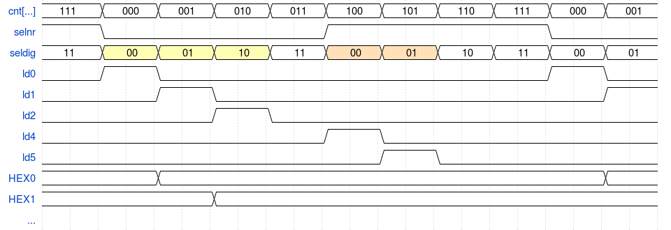
The output display configuration is stored in 5 registers which are updated cyclically, with a rate of around 100 Hz. In order to use one BCD converter and one BCD-to-segment converter, the input and accumulator values, and their digits are multiplexed digit by digit. A simple solution may be based on a counter from which 3 bits are used to generate the required control signals, as in the figure below: | |||
[[Fișier: appl11_mux_wave.png]] | |||
== Design hints == | == Design hints == | ||
Versiunea de la data 22 mai 2019 11:27
Requirement
Design, verify and implement a calculator. It adds, subtracts or multiplies an 8 bit number to/from the current content of its accumulator. It continuously display the input number (on the first two display digits) and the current content of the accumulator (on the last three digits of the display).
Description
The heart of the calculator is the FSM. It receives commands from the push buttons (PLUS, MINUS, MULTIPLY or CLEAR), and sends control signals to the datapath. Apart from the FSM there are 6 registers, one for storing the result (the accumulator), and one for each of the digits used for display. The inputs shown in red are the control signals generated by the FSM. The blocks colored in blue are sequential, clocked by the 50 MHz input clock and initialized/cleared by the common reset input. The reset is assimilated to the CLEAR command.
The output display configuration is stored in 5 registers which are updated cyclically, with a rate of around 100 Hz. In order to use one BCD converter and one BCD-to-segment converter, the input and accumulator values, and their digits are multiplexed digit by digit. A simple solution may be based on a counter from which 3 bits are used to generate the required control signals, as in the figure below:
Design hints
- For the BCD converter see Exercise 3 from Applications 4. Adapt that solution such that to convert an 8 bit binary number to a three digit BCD number.
- For the ROM module see Exercise 1 from Applications 8, or Applications 10
- The inputs bmul, bsub and badd from the push buttons, being active 0, may be transformed to single pulse internal signals, in order to easy the FSM design:
reg  button_d; // delayed button input
wire button_p; // one clock cycle pulse
always @(posedge clk)
    button_d = button;
assign button_p = button & ~button_d; // one clock cycle pulse generated after the push button was released

