Applications 8: Diferență între versiuni
Fără descriere a modificării |
Fără descriere a modificării |
||
| Linia 4: | Linia 4: | ||
The storage capacity is N x W bits, but the memory capacity may also be given in bytes. | The storage capacity is N x W bits, but the memory capacity may also be given in bytes. | ||
Being a vector of words or a bidimensional array of bits, the memory could be described using a single bidimensional variable, usually declared as | Being a vector of words or a bidimensional array of bits, the memory could be described using a single bidimensional variable, usually declared as a vector of multibit '''reg''' items. A memory array of N locations, with W bits per location is declared as: | ||
<syntaxhighlight lang = "verilog"> | <syntaxhighlight lang = "verilog"> | ||
reg [W-1: 0] memory [0: N-1]; | reg [W-1: 0] memory [0: N-1]; | ||
</syntaxhighlight> | </syntaxhighlight> | ||
'''Attention!''' | |||
* the width of the word is declared as usual, with msb as the left index, <syntaxhighlight lang="Verilog" inline>[msb:0]</syntaxhighlight> | |||
* the length of the memory is declared after the variable name, and starts with 0, the right index being the highest index of the vector, <syntaxhighlight lang="Verilog" inline>[0:endindex]</syntaxhighlight> | |||
Memories can also be classified by their synchronous or asynchronous character: | Memories can also be classified by their synchronous or asynchronous character: | ||
| Linia 18: | Linia 22: | ||
== Exercise 1 == | == Exercise 1 == | ||
=== ROM - Read-Only Memory === | === ROM - Read-Only Memory === | ||
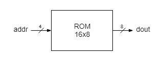
It may be described as a purely combinational logic circuit, whose output (data) is a logic function of its input (address). The transcoder from [[Applications 4#transcoder|Applications 4]] is nothing else than a ROM, with '''value''' input acting as an address that selects a particular location from where data is read and sent out as '''seg'''. There it was described behaviorally with a '''case''' statement that had a branch for each combination of input value bits. | |||
[[Fișier: appl8_rom.png]] | [[Fișier: appl8_rom.png]] | ||
A more flexible description employs a single memory array, declared as a vector of '''reg''' variables, and a statement that assigns the selected (addressed) element of the memory vector to the memory output. | |||
<syntaxhighlight lang = "verilog"> | |||
assign dout = memory[addr]; | |||
</syntaxhighlight> | |||
=== Memory initialization task === | === Memory initialization task === | ||
| Linia 61: | Linia 73: | ||
ff | ff | ||
</syntaxhighlight> | </syntaxhighlight> | ||
* Start a new project, '''rom''', in a newly created folder '''rom''' | |||
* Create a new verilog file ''rom.v'' that describes a 16x8 ROM using a vector variable and a continuous assignment. | |||
* Create a testbench, '''rom_tb''', that drives the input of '''rom''' with a sequence of addresses from 0 to highest one. Run simulation. | |||
* Open a text editor, write some values in binary format on successive lines, and save the file into the ''rom'' folder with the name ''meminit.txt'' | |||
* In the testbench module add an '''initial''' process with a single statement that calls the system task for memory initialization. Run simulation. | |||
* Assign the segments of Digit0 from DE1-SOC display to '''dout''', and SW[3] ... SW[0] switches to '''addr'''. | |||
* In the '''rom''' module add an '''initial''' process with a single statement that calls the system task for memory initialization. Compile the project and program the FPGA. | |||
== Exercise 2 == | == Exercise 2 == | ||
=== RAM - Read-Write Memory === | === RAM - Read-Write Memory === | ||
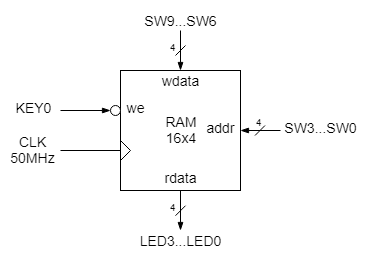
A synchronous memory reacts only on clock edges. The addresses are sampled at clock edges, the output changes also on clock edges, and the write is performed on clock edges too. | |||
[[Fișier: appl8_ram.png]] | [[Fișier: appl8_ram.png]] | ||
The FPGA has dedicated blocks for memory implementation, the so called ''ram blocks'', or ''ramblocks''. In order for the synthesis to map a memory description to a ''ramblock'', the sequential description must conform to a template: | |||
<syntaxhighlight lang="Verilog"> | |||
always @(posedge clk) begin | |||
if(~we) // if write is enabled, | |||
mem[addr] <= wdata; // update the addressed location to wdata value | |||
rdata <= mem[addr]; // data read from the address is transferred to the output | |||
end | |||
</syntaxhighlight> | |||
* Start a new project, '''ram''', in a newly created folder '''ram''' | |||
* Create a new verilog file ''ram.v'' that describes a 16x4 RAM using a vector variable and a sequential '''always''' process that assigns to '''rdata''' output the value of the memory location selected by '''addr'''. In the same process update the same location with '''wdata''' value if '''we''' input is active (active at '''0'''). | |||
* Create a testbench, '''ram_tb''', which writes some data to four addresses, and then reads the same addresses in the same order, as indicated in the waveforms below. Don't forget the clock! Run simulation and check the the written data are correctly read afterwards. | |||
[[Fișier: appl8_ram_wave.png]] | |||
* Assign LEDs to the output, switches to the '''addr''' and '''wdata''' inputs, a push button (KEY0) to the write enable input (the push button generates '''0''' if pressed), and a 50 MHz source clock to '''clk''' input. | |||
* Compile, program the FPGA and test the RAM. Set switches to an address and a write data, then push the write enable button. Change the address and data and push again the write enable button. Change back the address switches and see if the previously writtemn configuration reappears on LED. | |||
== Exercise 3 == | == Exercise 3 == | ||
=== Programmable display === | === Programmable display === | ||
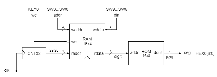
These application employs a dual port synchronous RAM. One port, the ''read port'', is used to read data ('''rdata''') from the memory, using the read address '''raddr'''. The other, the ''write port'', accesses the same memory array, but using another address, '''waddr''', to write '''wdata''' into. The write operation is performed only if the write enable pin ('''we''') is active (here it is active '''0'''). | |||
The data read from RAM is translated by the ROM into a 7 bit combination for the digit display. The RAM memory is read in sequence, address by address, changing the address at around each second. The sequence of 4 bit addresses are generated by a counter from which four suitable bits are chosen such that the rate of change is around 1 Hz. | |||
[[Fișier: appl8_ramrom.png]] | [[Fișier: appl8_ramrom.png]] | ||
* Start a new project, '''ramrom''', in a newly created folder '''ramrom''' | |||
* Copy the ''rom.v'' from Exercise 1 into this folder. | |||
* Copy the ''ram.v'' from Exercise 2 into this folder. Change it to a dual RAM. | |||
* Add '''cnt32.v''' to this project (you may reuse the '''cnt32''' module or file from the previous Application. | |||
* Create the top-level design file, ''ramrom.v''', and instantiate the modules and connect them as indicated. | |||
* Assign swithces, push button, clock source and digit display as shown. | |||
* Compile, program the FPGA, and play with the board switches and buttons. | |||
Versiunea de la data 17 aprilie 2019 06:10
A random access memory is an address based data storage block, with a highly regular structure, which may be logically defined either as a bidimensional array of bits, or a unidimensional list of data words. Each row of the array, or each item of the list has a unique address. The addresses form a contiguous set of integers, starting from zero and running up to the highest address which defines the size of the address space, usually a power of 2. The memory capacity is therefore the number of address locations, N, times the width of the memory location (or of the memory word), W. These two numbers are the main parameters of any memory:
- N - the number of address locations, also the number of words;
- W - the number of bits for each location, or the data word width;
The storage capacity is N x W bits, but the memory capacity may also be given in bytes.
Being a vector of words or a bidimensional array of bits, the memory could be described using a single bidimensional variable, usually declared as a vector of multibit reg items. A memory array of N locations, with W bits per location is declared as:
reg [W-1: 0] memory [0: N-1];
Attention!
- the width of the word is declared as usual, with msb as the left index,
[msb:0] - the length of the memory is declared after the variable name, and starts with 0, the right index being the highest index of the vector,
[0:endindex]
Memories can also be classified by their synchronous or asynchronous character:
- asynchronous - reading is done as soon as the order is presented;
- synchronous - all operations are synchronized by one of the clock signal fronts.
For physical implementation considerations, writing is always synchronous.
Exercise 1
ROM - Read-Only Memory
It may be described as a purely combinational logic circuit, whose output (data) is a logic function of its input (address). The transcoder from Applications 4 is nothing else than a ROM, with value input acting as an address that selects a particular location from where data is read and sent out as seg. There it was described behaviorally with a case statement that had a branch for each combination of input value bits.
A more flexible description employs a single memory array, declared as a vector of reg variables, and a statement that assigns the selected (addressed) element of the memory vector to the memory output.
assign dout = memory[addr];
Memory initialization task
Memory arrays may be initialized with predefined values from a text file using verilog system tasks $readmemb and $readmemh. $readmemb reads predefined values given in binary, while $readmemh is used if values are given in hexadecimal. These verilog system tasks have two mandatory arguments and two optional arguments, in the following order:
- initialization filename, given as a string (between double quotes)
- the memory array variable name
- the start address (optional)
- the end address (optional)
If the start and end addresses are not given, the memory array is initialized from the first address (address zero) until the last address or until the end of initialization file is reached.
If the memory initialization file, meminit.txt, resides in the project's folder, and the memory array to be initialized is mem inside the memory instance dut, the testbench may initialize the memory right at the beginning of the simulation:
initial $readmemb("../../meminit.txt", dut.mem);
If the initialization is intended to be done for the implemented memory, the initialization process must be placed inside the memory module, in which case the memory array name is just the variable array to be initialized:
initial $readmemb("../../meminit.txt", mem);
Memory initialization file
The initialization file is a text file with values written in binary (using 0 and 1 symbols) or in hexadecimal (using digits and letters a to f, either uppercase of lowercase). Values are separated by white spaces, tabs or newlines. Comments (started with // as in verilog) are ignored. An example of a binary initialization file:
// four values in binary text format
00000011
00001111
00111111
11111111
The same initialization sequence, but given as a hexadecimal text file:
// four values in hexadecimal text format
03
0f
3f
ff
- Start a new project, rom, in a newly created folder rom
- Create a new verilog file rom.v that describes a 16x8 ROM using a vector variable and a continuous assignment.
- Create a testbench, rom_tb, that drives the input of rom with a sequence of addresses from 0 to highest one. Run simulation.
- Open a text editor, write some values in binary format on successive lines, and save the file into the rom folder with the name meminit.txt
- In the testbench module add an initial process with a single statement that calls the system task for memory initialization. Run simulation.
- Assign the segments of Digit0 from DE1-SOC display to dout, and SW[3] ... SW[0] switches to addr.
- In the rom module add an initial process with a single statement that calls the system task for memory initialization. Compile the project and program the FPGA.
Exercise 2
RAM - Read-Write Memory
A synchronous memory reacts only on clock edges. The addresses are sampled at clock edges, the output changes also on clock edges, and the write is performed on clock edges too.
The FPGA has dedicated blocks for memory implementation, the so called ram blocks, or ramblocks. In order for the synthesis to map a memory description to a ramblock, the sequential description must conform to a template:
always @(posedge clk) begin
    if(~we)                   // if write is enabled,
        mem[addr] <= wdata;   //     update the addressed location to wdata value
    rdata <= mem[addr];       // data read from the address is transferred to the output
end
- Start a new project, ram, in a newly created folder ram
- Create a new verilog file ram.v that describes a 16x4 RAM using a vector variable and a sequential always process that assigns to rdata output the value of the memory location selected by addr. In the same process update the same location with wdata value if we input is active (active at 0).
- Create a testbench, ram_tb, which writes some data to four addresses, and then reads the same addresses in the same order, as indicated in the waveforms below. Don't forget the clock! Run simulation and check the the written data are correctly read afterwards.
- Assign LEDs to the output, switches to the addr and wdata inputs, a push button (KEY0) to the write enable input (the push button generates 0 if pressed), and a 50 MHz source clock to clk input.
- Compile, program the FPGA and test the RAM. Set switches to an address and a write data, then push the write enable button. Change the address and data and push again the write enable button. Change back the address switches and see if the previously writtemn configuration reappears on LED.
Exercise 3
Programmable display
These application employs a dual port synchronous RAM. One port, the read port, is used to read data (rdata) from the memory, using the read address raddr. The other, the write port, accesses the same memory array, but using another address, waddr, to write wdata into. The write operation is performed only if the write enable pin (we) is active (here it is active 0).
The data read from RAM is translated by the ROM into a 7 bit combination for the digit display. The RAM memory is read in sequence, address by address, changing the address at around each second. The sequence of 4 bit addresses are generated by a counter from which four suitable bits are chosen such that the rate of change is around 1 Hz.
- Start a new project, ramrom, in a newly created folder ramrom
- Copy the rom.v from Exercise 1 into this folder.
- Copy the ram.v from Exercise 2 into this folder. Change it to a dual RAM.
- Add cnt32.v to this project (you may reuse the cnt32 module or file from the previous Application.
- Create the top-level design file, ramrom.v', and instantiate the modules and connect them as indicated.
- Assign swithces, push button, clock source and digit display as shown.
- Compile, program the FPGA, and play with the board switches and buttons.


