Applications 2
Exercise 1 : 1 bit adder
Module declaration
Any Verilog circuit or block is enclosed within the keywords module and endmodule. The module keyword is followed by the name of the module. This name begins with a letter (Verilog is case-sensitive) or underscore (_), uses alphanumeric characters and underscores, and should be a meaningful one (adder, adder_32, counter, lshift_register, Serial_to_Parallel_converter, etc).
Right after the module name comes the interface description, a list of port declarations, separated by commas and enclosed within parentheses. It is strongly recommended to declare each port on a separate line, even if some ports have the same direction and size. Also it is recommended to group the declarations by their direction. A port declaration starts with the keyword that defines the port's direction: input or output. For one-bit ports the declaration comprises only the direction and the name. Port names follow the same naming rules used for module names. A port name should be a unique identifier inside the module's code - its scope is limited to the module.
A multi-bit port declaration defines the width of the port through two indices within brackets and separated by a colon: [msb:lsb]. The first index denotes the most significant bit (MSB), the second one is the least significant bit. MSB should always be greater than MSB. Usually the LSB index is 0, therefore if the width of the port is N, the first index would be N-1.
The module declaration comprises the keyword module, the module name and its interface, and ends with a semicolon:
module adder (            // keyword '''module''' followed by the module's name and the opening parenthesis of the interface
    input  logic a,       // one-bit input port named 'a'
    input  logic b,       // one-bit input port named 'b'
    output logic [1:0] s  // two-bit output port. Bit 1 is MSB, bit 0 is LSB. There is no comma after the last port declaration
);                        // the closing parenthesis of the interface and the semicolon that ends the module's declaration
Module description
Anything written between the module's declaration and the keyword endmodule is part of the module's description.
A module may be described by what it does. This is a behavioral description. Very simple modules could be described using a single instruction, that assigns to the output the result value of an expression over the inputs. Because Verilog is a description language, not a programming language, the assignments that describe how logic values are generated from other logic values are attached to special Verilog keywords. One such keyword is assign. It is followed by a single assignment: assign y = E(x1, x2, ... xN); It is forbidden to use the left-hand variable (y) inside the right-hand expression.
The one-bit adder may be described by a simple expression that computes the output value as the addition of its inputs:
assign s = a + b; // variable value s is always equal to the sum of a and b
The assign statement describes something that is continuously evaluated. It may be viewed as a small black box with an output and some inputs. The left-hand variable is updated immediately whenever any of the variables in the right-hand expression changes its value. The physical circuit that implements the assign statement is a combinational logic circuit (CLC) that reacts immediately to any change at its inputs.
The full code of the adder module:
module adder (
    input  logic a,
    input  logic b,
    output logic [1:0] s
);

assign s = a + b;

endmodule
Testbench module
The testbench is another module, therefore it is defined in a separate file. Also, the testbench is a simulation file - it cannot be synthesized and implemented. Always follow these rules:
- each module is defined in a separate file
- the name of the file is the name of the module, or closely resembles it
The testbench has no interface. All signals are generated internally. Therefore the testbench declaration has an empty interface list, module testbenchName();, or the parentheses may be missing at all, module testbenchName;
It is recommended to include in the name of the testbench the name of the module to be tested. The testbench for the adder module may be named adder_testbench, test_adder, adder_tb, a.s.o.
As for any module, the description follows the module declaration. The testbench instantiates the module to be tested and generates values for the signals connected to the inputs of the tested module. The testbench is used only in simulation, it cannot be synthesized. However, this restriction is turned to an advantage because the testbench may use procedural statements freely, as in ordinary programming languages, to generate whatever sequence of values for the stimuli is desired.
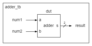
The DUT (device under test) is a block inside the testbench module. It is an instance of a module. The module is like a blueprint, while the instance is a materialization of that blueprint. For those familiar with object-oriented programming this may sound familiar. The module is like a class, and the instance is an object of that type.
A module instantiation starts with the moduleName followed by the instanceName and the list of its external connections enclosed within parentheses. Usually, the module instantiated in the testbench is named dut (device under test). The instance name should be a unique name inside the module where it's instantiated.
The list of connections connects each port of the instance to a signal of the testbench. It is strongly recommended to write each connection on a separate line. You may write the connections in the same order as in the interface declaration for that module. You should have at most ONE connection for each port, but some ports may be leaved unconnected if they are not used. A connection is declared with a dot (.) immediately followed by the name of the port and finally the name of the signal connected to that port, enclosed in parentheses: .modulePin(varName) . The connections in the list are separated by commas.
The adder module is instantiated with the name dut. Its inputs receive signals num1 and num2, and its output is connected to a wire named result:
adder dut (        // a module of type 'adder' is instantiated. The name of this instance is 'dut'
    .a  (num1  ),  // port 'a' is connected to signal 'num1'
    .b  (num2  ),  // port 'b' is connected to signal 'num2'
    .s  (result)   // port 's' is connected to 'result'. There is no comma after the last connection
);                 // the closing parenthesis of the interface and the semicolon that ends the module's instantiation
All signals and wires connected to an instance should be declared, and the declarations should precede the instantiation.
The signals connected to the instance inputs are stimuli generated by the testbench. They should be declared as variables of type reg. The instance outputs should be declared as variables of type wire. The variable declaration begins with the type (reg or wire) and ends with the variable's name. We strongly recommend to declare each variable in a separate line. Also, you should NOT initialize a variable in the declaration statement (keep in mind that Verilog is a description language, not a programming language). For the multi-bit signals the declaration must specify the width, in the same way you declare the width of a multi-bit port in the interface of a module.
logic num1;          // one-bit variable of type reg and named 'num1'
logic num2;          // one-bit variable of type reg and named 'num2'
logic [1:0] result;  // two-bit variable of type wire and named 'result'
As a rule of thumb, keep in mind that any output of an instance could be declared only as a wire, whereas the inputs to an instance are declared of type reg if you give them values using explicit assignment statements.
The stimuli for the adder block are generated as in Laboratory 1, using a Verilog initial block, inside which you assign values to signals num1 and num2. To thoroughly test the adder block it is useful to generate all possible combinations of values for those two signals. One such sequence of binary value pairs may be 00, 01, 10, 11:
initial begin
       num1 = 1'b0; num2 = 1'b0; // begin with both adder inputs zero
    #5 num1 = 1'b0; num2 = 1'b1; // after a delay, change the value of one input of the adder
    #5 num1 = 1'b1; num2 = 1'b0; // go to the next combination of values
    #5 num1 = 1'b1; num2 = 1'b1;
    #5 $stop;
end
Note: as in Laboratory 1, you may generate the values for num1 and num2 in a single statement, combining them into one two-bit bundle (for example
{num1, num2} = 2'b01;
)
The full code of the adder testbench module:
module adder_tb;

// declarations
logic num1;
logic num2;
logic [1:0] result;

// instantion
adder dut (
    .a  (num1  ),
    .b  (num2  ),
    .s  (result)
);

// stimuli generation
initial begin
       {num1, num2} = 2'b00;
    #5 {num1, num2} = 2'b01;
    #5 {num1, num2} = 2'b10;
    #5 {num1, num2} = 2'b11;
    #5 $stop;
end

endmodule
Module simulation
Simulate the adder_tb testbench and check on the waveforms that the output of the adder module is indeed the sum of its input values.
Exercise 2 : 2 bit adder
design module
The 2 bit adder has almost the same interface as the 1 bit adder. All names are the same, only their widths are different. The inputs are 2 bits wide, the output has 3 bits, to accommodate the biggest possible result (3 + 3 = 6). Since the description is high-level, employing the add operator, it is exactly the same as for the previous adder.
module adder2 (
    input  logic [1:0] a,
    input  logic [1:0] b,
    output logic [2:0] s
);

assign s = a + b;

endmodule
simulation module
The 2 bit adder module has two inputs of 2 bits each. That means there are more input combinations to be tested, actually 16 (4 values for the one input, and 4 values for the other one). To run through all those 16 combinations the pair of statements num1 =value1; num2 =value2; may be employed 16 times with different values. If the combinations are generated in a systematic way (for example in the increasing order of the input values), a for statement is more convenient.
module adder2_tb;

// declarations
logic [1:0] num1;
logic [1:0] num2;
logic [2:0] result;

// instantion of a 2 bit adder
adder2 dut (
    .a  (num1  ),
    .b  (num2  ),
    .s  (result)
);

// stimuli generation
int i; // integer type variable used to control the for loop
initial begin
    {num1, num2} = 0;                       // initial values of the adder2 inputs
    for(i = 0; i < 16; i = i + 1)           // the control variable runs from 0 to 15. After the last iteration it is incremented (again) to 16 and the loop is terminated.
        #5 {num1, num2} = {num1, num2} + 1; // a nonzero delay is mandatory to ensure that each combination lasts at least one simulation step.
    #5 $stop;
end

endmodule
Implementation
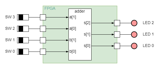
To implement the adder on the FPGA and to interact with it we should imagine some means to set and to change the adder input values and to see the value of its output. The FPGA board allows us to interact with the circuit implemented inside the FPGA through switches, push buttons and various LEDs that are connected to FPGA pins, which may be configured to be wired inside the FPGA to the ports of the implemented module. The FPGA pins assignment is done through the constraints file. For each pin assignment there is a line that instructs the implementation tool to connect the port with a given name to a particular FPGA pin, and also sets the parameters of the I/O pad of that pin. For example
set_property -dict { PACKAGE_PIN T2 IOSTANDARD LVCMOS33 } [get_ports { a[1] }];is a constraint that connects the first bit of a input to the FPGA pin labelled T2.
Note: For each FPGA board you may find constraints files with constraints for all FPGA pins, with indications as to which switch, button, LED, a.s.o. is connected to which FPGA pin. All constraints are commented. You should uncomment only the lines for the switches, buttons, LEDs a.s.o. that you want to use, and replace the port names with the names of ports from your module. For multi-bit ports there must be one separate connection constraint for each port bit, since each port bit needs a separate FPGA pin.
The 2 bit adder will be tested using four switches to set the input values, and three LEDs to show the output 3-bit value:
##Switches
set_property -dict { PACKAGE_PIN T2   IOSTANDARD LVCMOS33 } [get_ports { a[1] }]; #SW 3
set_property -dict { PACKAGE_PIN U1   IOSTANDARD LVCMOS33 } [get_ports { a[0] }]; #SW 2
set_property -dict { PACKAGE_PIN U2   IOSTANDARD LVCMOS33 } [get_ports { b[1] }]; #SW 1
set_property -dict { PACKAGE_PIN V2   IOSTANDARD LVCMOS33 } [get_ports { b[0] }]; #SW 0

##LEDs
set_property -dict { PACKAGE_PIN G1   IOSTANDARD LVCMOS33 } [get_ports { s[0] }]; #LED 0
set_property -dict { PACKAGE_PIN G2   IOSTANDARD LVCMOS33 } [get_ports { s[1] }]; #LED 1
set_property -dict { PACKAGE_PIN F1   IOSTANDARD LVCMOS33 } [get_ports { s[2] }]; #LED 2
Exercise 3
design and verify in simulation a 2 by 2 bit multiplier. The output has 4 bits, to cover the whole range of the multiplication. The biggest output value is 9 (= 3 x 3). The description is behavioral, using the multiplication operator.
Exercise 4
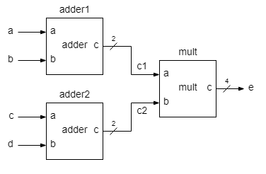
Design a source file for top-level entity. It instantiates two 1 bit adder modules (desined in Exercise 1) and one multiplier module from Exercise 3. The whole circuit has a multilevel hierarchy with mixed description: the top-level has a structural description, while the low-level blocks have behavioral descriptions.
Note: If two or more instances of the same module appear inside another module description, they should have distinct instance names. Each instance should be uniquely identified.
Note: The structural description has instances and wires that connect the instances between them, and to the ports.
Write a testbench source file for the top-level entity.


