DIC Lab Work 0
De la WikiLabs
Jump to navigationJump to searchNotions and Knowledge Required
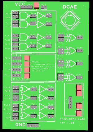
Development board
In this lab you will use a development board equipped with digital integrated circuits that offers the following logical functions:
- 4 gates NAND, whose outputs are inversely connected, so they can be used as gate AND
- 4 NOR gates, whose outputs are inversely connected, so they can be used as gateways OR
- 4 XOR gates
- 4 logical inputs selectable by a jumper, and equipped with one LED indicating the logical value selected (LED illuminated for 1 logic, off for 0 logic)
- 4 VCC connections (VDC of 5V)
- 4 GND connections
- 4 LEDs that can be used to view the logic value of any point in the circuit (LED illuminated for 1 logic, off for 0 logic)
Rules for using the development board:
- The board must be powered using a USB cable connected to the computer so that the power LED is on
- The outputs of a gate can be connected to the inputs of another gate by wire, which will be made available together with the development board
- The outputs of two gates will not be connected
- Note that each logical gate input has two pins, one of which maximum will be connected to the output of a logic gate, the other one can be connected to the input of a logical gate
- Inverters on the board have already connected the inputs to the outputs of the AND /NO /NO-NO gates, so the pins on the inverter inputs can not be used to link the inputs of the inverters with the output of another gate on the board.
- The reversing function can also be implemented via the AND-NU or XOR gates on the board
- Do not connect gate outputs to VCC or table
The wiring diagram of the development board is available here: Fișier:Placa integrate cid proiect.pdf
Example
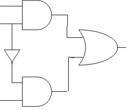
A selection circuit (multiplexer) using the development board will be implemented with the help of the teacher if necessary:
- Use gate combinations NAND / NOR and inverter to make gate AND / OR circuit diagram.
- An AND gate will be used to implement the inverter from the circuit diagram, linking both gate inputs AND NOT to the signal to be reversed.
- The circuit output will be connected to one of the LEDs to view its logic value
- We will build, by experimenting, the truth table of the selection circuit
Requirements
Students will implement a circuit to choose the teacher, consisting of 4-5 interconnected logic grids using the development board, and obtain the circuit truth table either by analyzing the logic scheme or by measuring its implementation on the development board.

