DIC Seminar 4
The Counter is one of the most used digital circuits and surely one of the best known outside the world of electronics. Any microprocessor has a program counter ("program counter") without which it can not run the programs on the computer. The program counter generates a sequence of memory addresses in ascending order, one in each clock period, and occasionally when a jump in the program jumps to an address other than the next one.
Example 1
The simplest count is the increment register. Exercise 4 in Seminar 2 required a description of a combined incremental command circuit, one of the possible variants being:
module increment (
     input inc,
     input [3: 0] and,
     output reg [3: 0] out)

always @ (*)
     out = inc? a + 1: a;
endmodule
With minimal modifications, the above description can be converted to a commanded increment counter. To generate an increasing sequence of numbers, the output number is returned to the input. The loop can be closed inside the module, giving up the input of:
module incorrect (
     input inc,
     output reg [3: 0] out
     )

always @ (*)
out = inc ? out + 1: out; //infinite loop!

endmodule
Closing a loop over a combinational circuit often leads to an unstable circuit, and in the case of the above description the simulation will go into an infinite loop. Please note, therefore, a design rule:
Buildings like
out = inc ? out + 1: out;
or
out <= inc? out + 1: out;
can not be used in a combination description block, either assign or always @ (*) .
The loop can only be closed over a combinational circuit and a register, obtaining a sequential circuit. Therefore, we will always convert the block from a combinational one (sensitive to any change of the variables in the right-hand expressions) into a sequential one, sensitive only to the active edge of the clock signal (1). The clock signal must be declared as input (2). And, very importantly, the assignment in the sequential block is obligatory nonblocking /non-blocking (3), a basic rule in the description of sequential circuits (see example 2 of seminar 3):
module counter (
input clk, //<- obs. 2
input inc,
output reg [3: 0] out
)

always @ (posedge clk) //<- obs. 1
out <= inc? out + 1: out; //<- obs. 3

endmodule
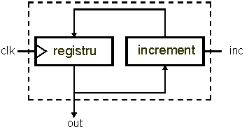
The above description is equivalent to the following block scheme:
Write a test module of the counter module that generates the clock and command signal, initially inactive, then active, and simulate the circuit. What's on his way out? "
The above description is synthesizable and the synthesized counter works flawlessly. And yet at simulation the output is indefinitely indefinite. The reason is the initial value of the reason. Any update of the out variable is based on its previous value, and the first execution of the assignment instruction ( out <= inc? Out + 1: out; ) takes into account the initial value. Value that is undefined, ie x! Gathering 1 at an undefined value also gives an undefined value. Simulation is, however, only an approximation of reality, and we need to be aware of its limitations.
An artifact to initialize the out variable would be forcing its value out of the module from the test module.
During verification, we can have direct access to any (variable) signal inside the tested module if we use its full name, unique name within the block hierarchy in the structure of the tested module. The full name is specified as the name of a variable in a hierarchy of objects in a program written in an object-oriented language:
topInstanceName.signal

topInstanceName.blockInstanceName.signal

topInstanceName.blockInstanceName.subblockInstanceName.signal
In the case of our counter, if in the test module it is instantiated with the uut name, the out variable can be initialized in step 0 of the simulation directly from the test module:
initial uut.out=0;
This mode of access should be used with parsimony and only in test modules, not a synthesized statement! It is recommended to use direct access only for the purpose of reading (monitoring) variables that we do not have direct access through the top court interface. Assignments through direct access must be strictly limited to situations where we know very clearly all the effects it produces. note:
Much more elegant is to design the counter with a reset or clear input, a practical input whenever we want to bring the numerator to zero. Initializing the counter will be done by activating the delete entry.
Example 2
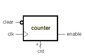
Add the numerator a synchronous reset (often called clear) input in 0. Check the circuit using the same test module in which you start the reset input for at least one clock time at the beginning of the simulation.
The activation input of the count (entry inc in example 1) is usually called enable or count enable ('ce' , 'cen').
To check the entire counting sequence, let the simulation "run" for more than 16 clock periods when the enable command is activated. We can use a clock delay calculated in the test module, for example #170 if the clock time is 10 or, more conveniently, we can expect a precise number of active clock fronts using the ' repeat ':
repeat (17) @ (posedge clk);
repeat (n) repeatedly executes the execution of the attached instruction block. In the above case, repeat 16 times the active front of the clock. The advantage of this instruction is that we do not depend on the absolute value of the clock.
Observe how the count is "overhead" after reaching the maximum value (15), resuming the counting from zero (increments modulo 16).
Example 3
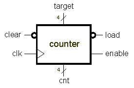
Behaviorally describe a synchronous synchronous 4-bit counter with a synchronous load, a countdown input, and a deletion input. Load command ( load ) and delete ( clear ) are active in zero. All controls act only synchronously with the clock. If multiple command inputs are active at the same time, the highest priority input determines the next output value. In descending order of priority, the commands are: "clear, load, enable.
The charging input is active in 0. When it is active, the active clock front causes the counter to load the value on the target entry. All functions of this counter can be arranged in a table:
1 || 1 || 1 || cnt + 1 || counting| clear | load | enable | cnt + | function |
| 0 | X | X | 0 | deletion |
| 1 | 0 | X | target | loading |
| 1 | 1 | 0 | cnt | memorization |
In the table above, the value X at some inputs means that the logical value of those entries does not matter ( do not care ). The truth table can thus be substantially compressed. For example, when the reset input is inactive ( clear == 1 ) and charging is enabled ( load == 0 ), the numerator loads ('target' value) the enable entry. The two value combinations on the control inputs 100 and 101 are collapsed in one, 10X. This compaction can also be used in Verilog table constructions, such as the 'case' instruction. In order to use the X value in specifying the cases of the instruction, the alternative casex, which has the same format as the 'case' instruction (see example 4 in the seminar 2), must be used:
casex (expression_case)
    value1: instruction1
    ...
    default: instruction
endcase
Unlike the 'case' construction, which admits only precise numerical values for each case, the casex construction allows some bits to be undefined in some cases. For example, the previously analyzed case can be described in Verilog as follows:
3'b10X: out <= target;
Check circuit functionality for all combinations of control signal values.
Exhaustive generation of all combinations of control signal values is most convenient in a 'for' type cycle, in which we treat the value combination as a binary number that we initialize zero at the beginning of the test sequence and then we increment it at each iteration. The instruction 'for' has in Verilog the same format as in C or in Java:
    for (initializations, stop condition, iteration end assignments)
        block of instructions
such as
    for (index=0; index <8; index=index + 1)
    begin
        {clear, load, enable}=index;
        repeat (16) @ (posedge clk);
    end
We can control the loop control for an integer index that increments iteration with iteration to the desired value. In the test module, we can declare and use integer variables as in programming languages, but these variables are not signals:
integer index;
An iteration of the 'for' loop above takes 16 clock periods for each combination of values tested. Observe the compact mode that assigns values to the three signals. Instead of individual assignments, the three signals were grouped into a 3-bit vector which is then assigned a full value. The last three bits of the binary representation of the value of the 'index' variable will be assigned to the three signals. Grouping of signals in Verilog is possible thanks to the concatenation operator:
{clear, load, enable}
The number of bits of the new variable is the sum of the bits of the grouped variables, and the bits are arranged in the order of concatenation of the variables. In our case, 'clear' is the significant bit (MSB) of the control signal vector.
Example 4
Using the previous counter, perform a controllable frequency divider, the divider being selectable so that the output frequency is 1/2, 1/4, 1/8 or 1/16 of the clock frequency.
At the instantiation of the counting module, make sure that all inputs are connected either to a signal generated in the test mode, either to the mass (at 0) or to the feed (at value 1). Only those inputs that do not affect the operation of the circuit can be left unconnected ("empty" or "floating"). In our example, the 'target' entry can be neglected because the numerator will never load. In general, however, unconnected entries can result in erroneous results due to their undefined value (X). A rule that relieves you of surprising simulations and syntheses:
Homework
Implement a pulse generator with controlled frequency and fill factor. The generated signal period will be equal to a multiple of the clock, Tw=Tclk * tw, and the duration of the pulse is controlled by another input, Tp=Tclk * tp.
- using the numerator of Example 3;
- using a purely behavioral description;


