Diferență între revizuiri ale paginii „DIC Lab Work 5”
De la WikiLabs
Jump to navigationJump to searchCbira (discuție | contribuții) |
Cbira (discuție | contribuții) |
||
| Linia 12: | Linia 12: | ||
* It will describe in Verilog a 16x4b RAM with a read-write port. Reading is synchronous. | * It will describe in Verilog a 16x4b RAM with a read-write port. Reading is synchronous. | ||
| − | * The necessary | + | * The necessary pin connections will be written |
| − | ** | + | ** the address to SW7-4 and date of entry to SW3-0. |
| − | ** | + | ** the write enable signal at one of the buttons (KEY0 ... KEY3). |
| − | ** | + | ** the output at LEDR3-0. |
** memory clock input to one of the DE1 plate oscillators. | ** memory clock input to one of the DE1 plate oscillators. | ||
| − | * | + | * Program the FPGA, and using the switches and buttons on the board, write 3, 6, and 10 with the values 2, 1 and 7, then read them in the same order. Notice, using the LEDs of the board, if the memory has been written. |
== Exercise == | == Exercise == | ||
Versiunea de la data 30 mai 2018 09:34
Required Notions and Knowledge
- Boolean logic and numbering systems
- Verilog Syntax Verilog_EN
- Using the Altera Quartus II Synthesis Program
- List of pins for DE1 board, List of pins for DE1-SoC board
- Sequential Circuits
- Counter
- RAM Memory
Example
- It will describe in Verilog a 16x4b RAM with a read-write port. Reading is synchronous.
- The necessary pin connections will be written
- the address to SW7-4 and date of entry to SW3-0.
- the write enable signal at one of the buttons (KEY0 ... KEY3).
- the output at LEDR3-0.
- memory clock input to one of the DE1 plate oscillators.
- Program the FPGA, and using the switches and buttons on the board, write 3, 6, and 10 with the values 2, 1 and 7, then read them in the same order. Notice, using the LEDs of the board, if the memory has been written.
Exercise
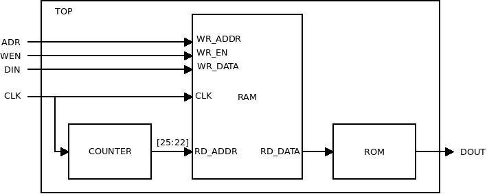
- Describe in Verilog a 16x4b RAM with two ports:
- A write-only sync port with the following signals:
- WR_ADDR - the address you write
- WR_EN - write command
- WR_DATA - written data
- A read-only read-only port with the following signals:
- RD_ADDR - read address
- RD_DATA - read data
- A write-only sync port with the following signals:
- The memory will be instantiated in the TOP module as shown below:
module COUNTER (
    input clk,
    output reg [31: 0] cnt
);

always @ (posedge clk) cnt <= cnt + 1;

endmodule

module ROM(
    input [3: 0] in,
    output reg [3: 0] out
);

always @ (in)
    case (in)
        0: out=4'b1010;
        1: out=4'b0110;
        2: out=4'b0011;
        3: out=4'b1110;
        4: out=4'b1011;
        5: out=4'b1111;
        6: out=4'b0111;
        7: out=4'b1100;
        8: out=4'b0001;
        9: out=4'b0101;
        10: out=4'b1101;
        11: out=4'b0000;
        12: out=4'b0010;
        13: out=4'b0100;
        14: out=4'b1000;
        15: out=4'b1001;
    endcase

endmodule
- Write the constraints required to connect the TOP module ports:
- DIN to SW7-4,
- ADR at SW3-0,
- WEN la KEY3,
- DOED to LEDR3-0,
- clock input at CLOCK_50.
- Schedule the FPGA board; Write the RAM with the values required to produce DOUT a sequence of numbers indicated by the teacher.
Submission of Exercises
For scoring, the following files will be submitted to the e-mail address indicated by the teacher.
An archive zip
- All Verilog files (with the .v extension) containing the circuit description
- A constraint file with the .qsf extension
- A Quartus project file with the .qpf extension
Note that the archive will only contain files (without directories).
The subject of the email message must follow the [Name] _ [First Name] _ [Group] _Mem example Popescu_Ion_423B_Mem
